Amorphous silicon doped with fluorine for selectors of resistive random access memory cells

a random access memory and amorphous silicon technology, applied in the field of amorphous silicon doped with fluorine for selectors of resistive random access memory cells, can solve the problems of difficult to form high density memory arrays, difficult to form diodes and transistors, and negatively affecting other components of reram cells, so as to reduce leakage and increase the band gap

Active Publication Date: 2015-11-03
INTERMOLECULAR
View PDF5 Cites 6 Cited by
  • Summary
  • Abstract
  • Description
  • Claims
  • Application Information

AI Technical Summary

Benefits of technology

[0004]Provided are resistive switching memory cells having selectors and methods of fabricating such cells. A selector may be disposed between an electrode and resistive switching layer. The selector is configured to undergo an electrical breakdown when a voltage applied to the selector exceeds a selected threshold. For purposes of this disclosure, the breakdown is defined as a reversible process associated with a rapid change in resistance of the selector. Various aspects of this process are further described below in particular with reference to FIGS. 3C-3E. The selector is formed from amorphous silicon doped with fluorine. The concentration of fluorine may be between about 0.01% atomic and 3% atomic, such as about 1% atomic. Amorphous silicon has a larger band gap than, for example, crystalline silicon and, therefore, has a lower leakage. Dangling bond and weak bond states appearing in the mid-gap position of amorphous silicon are eliminated by adding fluorine. Fluorine binds to and passivates defects. In some embodiments, a fluorine reservoir is positioned in a low current density region of the memory cell to counter diffusion of fluorine from the selector into other components.

Problems solved by technology

However, diodes and transistors are complex and often bulky components that require many processing steps and make it difficult to form high density memory arrays.
Some processing operations, such as diode activation at a high temperature (e.g., about 750° C.) may negatively impact other components of ReRAM cells further complicating cell design and fabrication.
While the direct gap in crystalline silicon satisfies this criterion, crystalline silicon has high leakage in the off-state and high coupling to phonons.
Furthermore, crystalline silicon is generally harder to integrate into ReRAM cells.
However, polysilicon has undesirable grain boundary leakage.
However, pure amorphous silicon still has a high leakage in the off-state due to localized dangling bond states and weak bond states that appear inside the energy gap of amorphous silicon.
These localized states lead to substantial leakage in part because of trap assisted tunneling.
For example, nitrogen may not be as effective as fluorine in passivating defects because each nitrogen atom needs to form three covalent bonds while the defect geometry may allow for one or at most two states.
Chlorine may also be not as effective as fluoride because its large atomic creates large elastic strain fields thereby decreasing chlorine incorporation.
Yet another example, hydrogen may be less effective than chlorine or fluorine because hydrogen exhibits low barriers for breaking the bond with the passivated atom and for diffusion that can lead to device degradation.
Insufficient amount of fluorine atoms will result in incomplete passivation and the selector will retain its leakage.
On the other hand, introducing too much fluorine into amorphous silicon may create interstitial states.
Post-deposition annealing can reduce the number of defects and thus decrease the required amount of fluorine, however, high annealing temperatures (e.g. such as above 750° C.) can cause a transformation of amorphous silicon into a crystalline form.
Without being restricted to any particular theory, it is believed that high electrical fields developed across the doped selector during its operation may cause degradation.
In particular, degradation may be due to diffusion of fluoride ions formed in the selector during its fabrication.
As such, the selector may be depleted with from fluoride ions and may start exhibiting leakage as described above.
That is, defects may travel through an interface formed by this electrode with the resistive switching layer (i.e., the reactive interface).
Furthermore, there may be some mobility of defects within resistive switching layer 104.
This breakage generally does not correspond to complete dispersion of defects forming these conductive paths and may be a self-limiting process, i.e., the process may stop after some initial breakage occurs.
In general, a selector that is less than 5 nm thick is too leaky, while a selector thicker than 200 nm is too bulky for modern devices.

Method used


Image

  • Amorphous silicon doped with fluorine for selectors of resistive random access memory cells
  • Amorphous silicon doped with fluorine for selectors of resistive random access memory cells
  • Amorphous silicon doped with fluorine for selectors of resistive random access memory cells

Examples


Embodiment Construction

[0022]A detailed description of various embodiments is provided below along with accompanying figures. The detailed description is provided in connection with such embodiments, but is not limited to any particular example. The scope is limited only by the claims and numerous alternatives, modifications, and equivalents are encompassed. Numerous specific details are set forth in the following description in order to provide a thorough understanding. These details are provided for the purpose of example and the described techniques may be practiced according to the claims without some or all of these specific details. For the purpose of clarity, technical material that is known in the technical fields related to the embodiments has not been described in detail to avoid unnecessarily obscuring the description.

INTRODUCTION

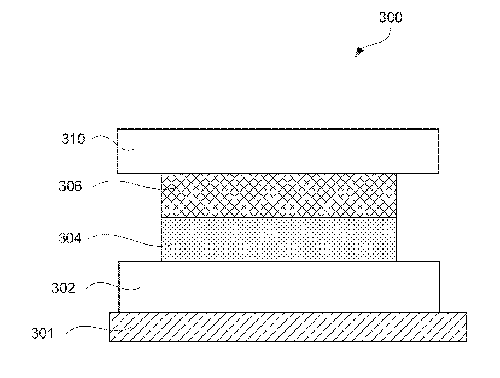
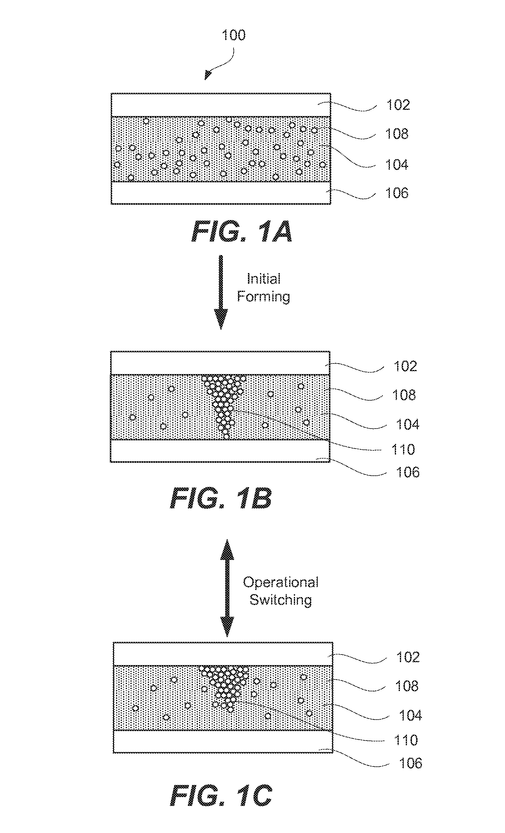
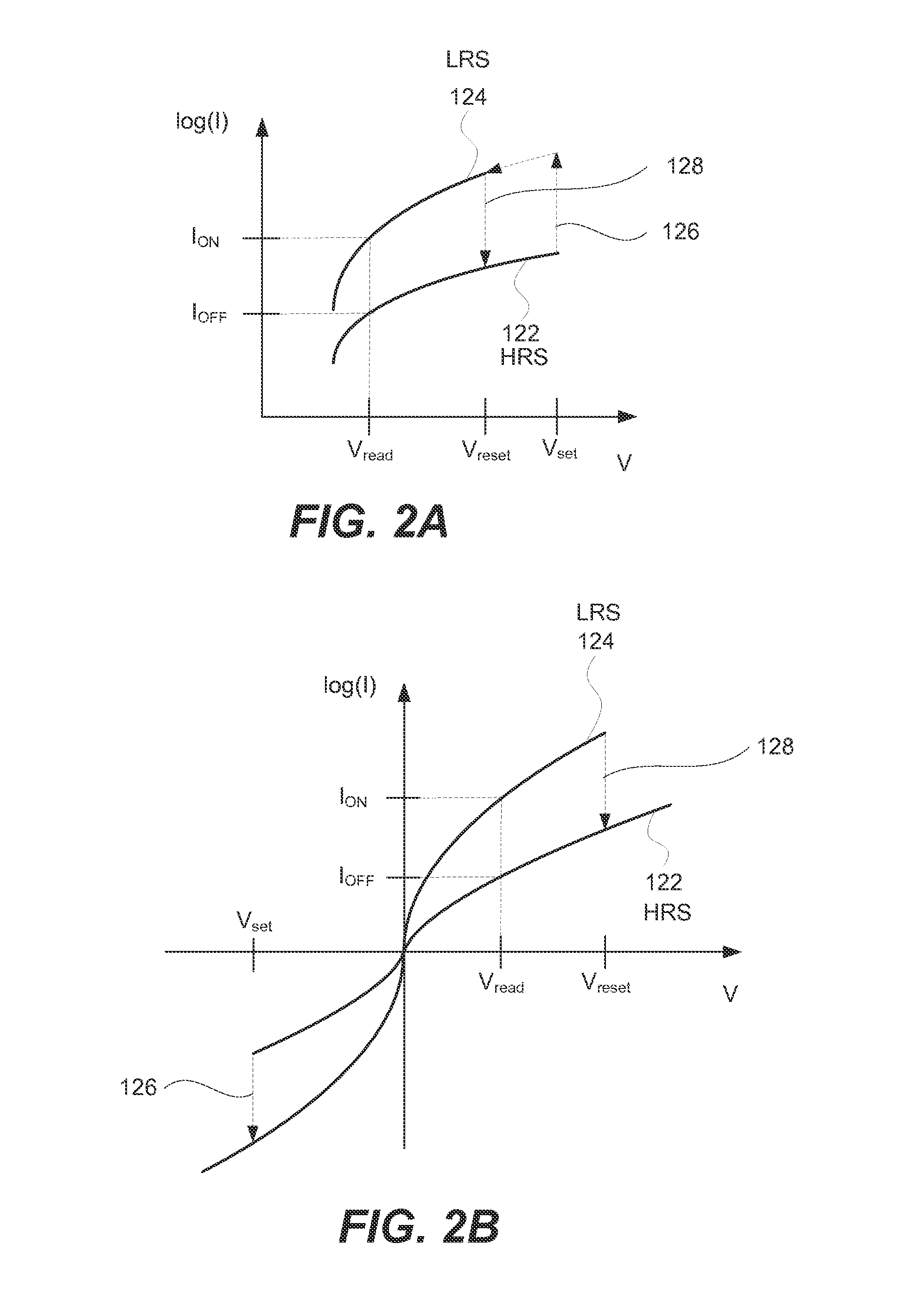
[0023]A ReRAM cell exhibiting resistive switching characteristics generally includes multiple layers formed into a stack, such as a “metal-insulator-metal” (MIM) stack...


PUM


Abstract

Provided are resistive switching memory cells having selectors and methods of fabricating such cells. A selector may be disposed between an electrode and resistive switching layer. The selector is configured to undergo an electrical breakdown when a voltage applied to the selector exceeds a selected threshold. The selector is formed from amorphous silicon doped with fluorine. The concentration of fluorine may be between about 0.01% atomic and 3% atomic, such as about 1% atomic. Amorphous silicon has a larger band gap than, for example, crystalline silicon and, therefore, has a lower leakage. Dangling bond and weak bond states appearing in the mid-gap position of amorphous silicon are eliminated by adding fluorine. Fluorine binds to and passivates defects. In some embodiments, a fluorine reservoir is positioned in a low current density region of the memory cell to counter diffusion of fluorine from the selector into other components.

Description

BACKGROUND[0001]Nonvolatile memory is computer memory capable of retaining stored information even when unpowered. Non-volatile memory is typically used for secondary storage or long-term persistent storage and may be used in addition to volatile memory, which loses the stored information when unpowered. Nonvolatile memory can be permanently integrated into computer systems (e.g., solid state hard drives) or can take the form of removable and easily transportable memory cards (e.g., USB flash drives). Nonvolatile memory is becoming more popular because of its small size / high density, low power consumption, fast read and write rates, retention, and other characteristics.[0002]Flash memory is a common type of nonvolatile memory because of its high density and low fabrication costs. Flash memory is a transistor-based memory device that uses multiple gates per transistor and quantum tunneling for storing the information on its memory device. Flash memory uses a block-access architecture...

Claims


Application Information

Patent Timeline
Patent Type & Authority Patents(United States)
IPC IPC(8): H01L23/52H01L23/528
CPCH01L23/528G11C13/0007G11C13/003G11C2213/33G11C2213/71G11C2213/73H01L2924/0002H10B63/20H10B63/80H10B63/84H10N70/24H10N70/8833H10N70/826H01L2924/00H10B63/24
Inventor BARABASH, SERGEYPRAMANIK, DIPANKAR
Owner INTERMOLECULAR
Why Eureka
Try Eureka