Amorphous oxide and field effect transistor

a field effect transistor and oxide technology, applied in the direction of basic electric elements, electrical equipment, semiconductor devices, etc., can solve the problems of variable tft characteristics, and achieve excellent field-effect mobility, excellent transistor characteristics, and excellent s value

Active Publication Date: 2012-07-03
CANON KK
View PDF33 Cites 105 Cited by
  • Summary
  • Abstract
  • Description
  • Claims
  • Application Information

AI Technical Summary

Benefits of technology

[0010]The present invention has been made in view of the above-mentioned problems. Therefore, an object of the present invention is to provide an amorphous oxide and a field-effect TFT which have excellent transistor characteristics including an excellent field-effect mobility and an excellent S value, excellent environmental stability, and a high margin of atomic composition ratios (degree of freedom of design).
[0014]According to an embodiment of the present invention, the amorphous oxide which has excellent semiconductor characteristics can be obtained. Further, the field effect transistor which has excellent transistor characteristics including an excellent field-effect mobility and an excellent S value, and excellent environmental stability can be provided. Further, the field effect transistor which has a high margin of atomic composition ratios (degree of freedom of design) can be provided, which has the transistor characteristics with little variance depending on the atomic composition ratios of atoms (especially metallic atoms) forming the field effect transistor.

Problems solved by technology

488-492) has a problem that, depending on the atomic composition ratios of the metallic elements mainly forming the non-crystalline oxide film used as the active layer, the TFT characteristics vary greatly.

Method used


Image

  • Amorphous oxide and field effect transistor
  • Amorphous oxide and field effect transistor
  • Amorphous oxide and field effect transistor

Examples


example 1

(Comparative Evaluation of Example 1 and Comparative Examples 1 and 2)

[0086]With regard to the In—Zn—O active layer with Mo added thereto obtained in Example 1, the optical absorption spectrum was analyzed. Band gap of the above-mentioned oxide film with Mo added thereto was about 2.7 to 2.9 eV depending on the atomic composition ratio of In, which is substantially the same as those of the In—Zn—O film of Comparative Example 1 and the In—Zn—O film with Mo added thereto of Comparative Example 2.

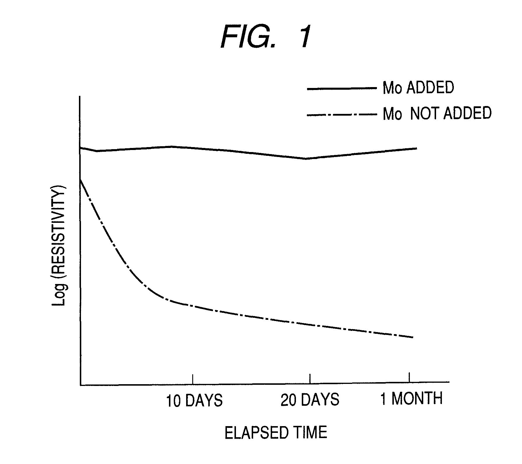
[0087]Next, in order to review the stability over time of the In—Zn—O film with Mo added, the oxide films manufactured in Example 1 and Comparative Examples 1 and 2 were left at rest in an atmosphere at a temperature of 20° C. and at a humidity of 50%, and the variations over time of the resistivity were measured. With regard to the oxide films of Comparative Examples 1 and 2, after being left at rest for a month, the resistivity decreased substantially by an order to two orders of magnitude d...

example 2

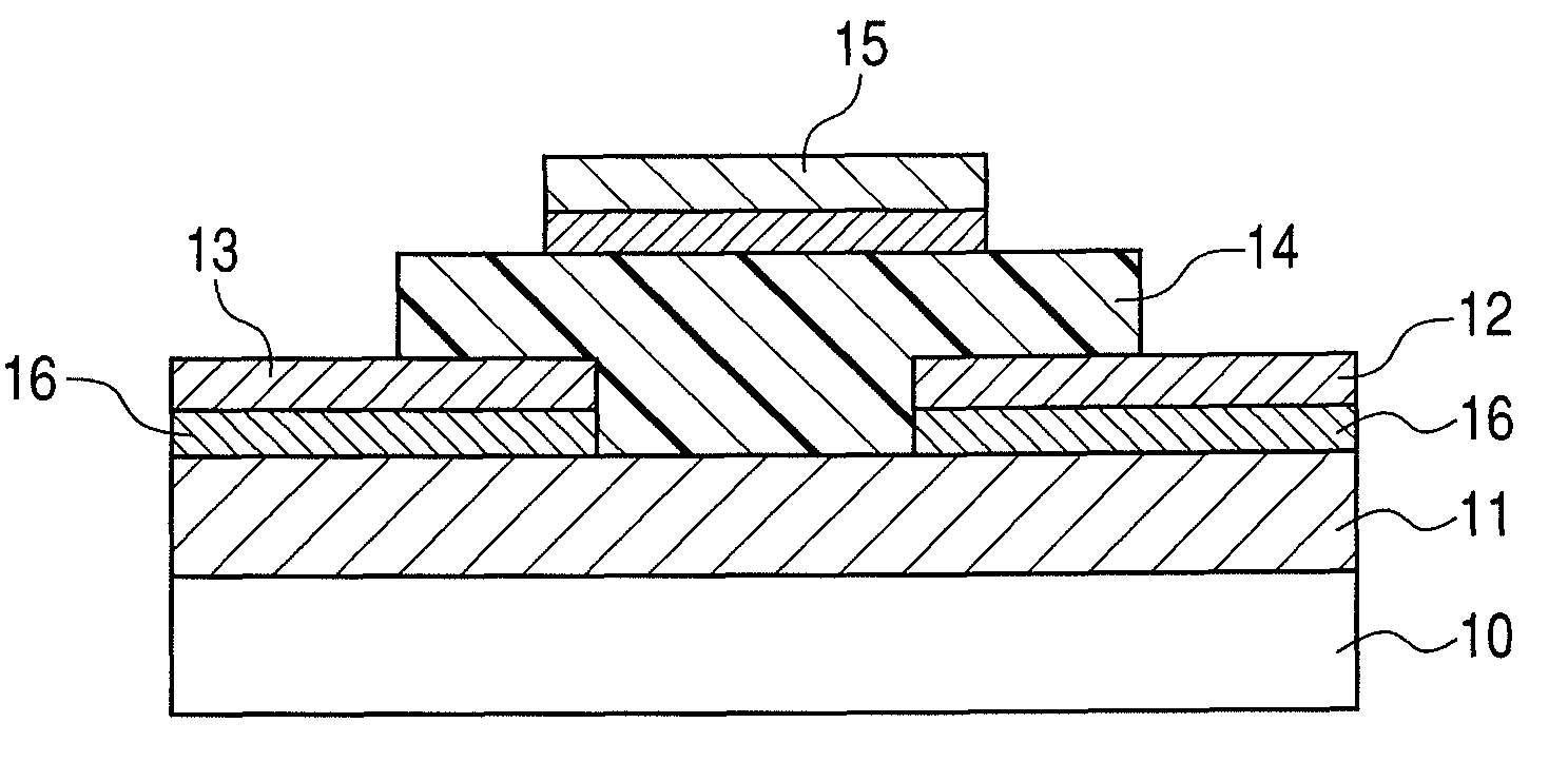
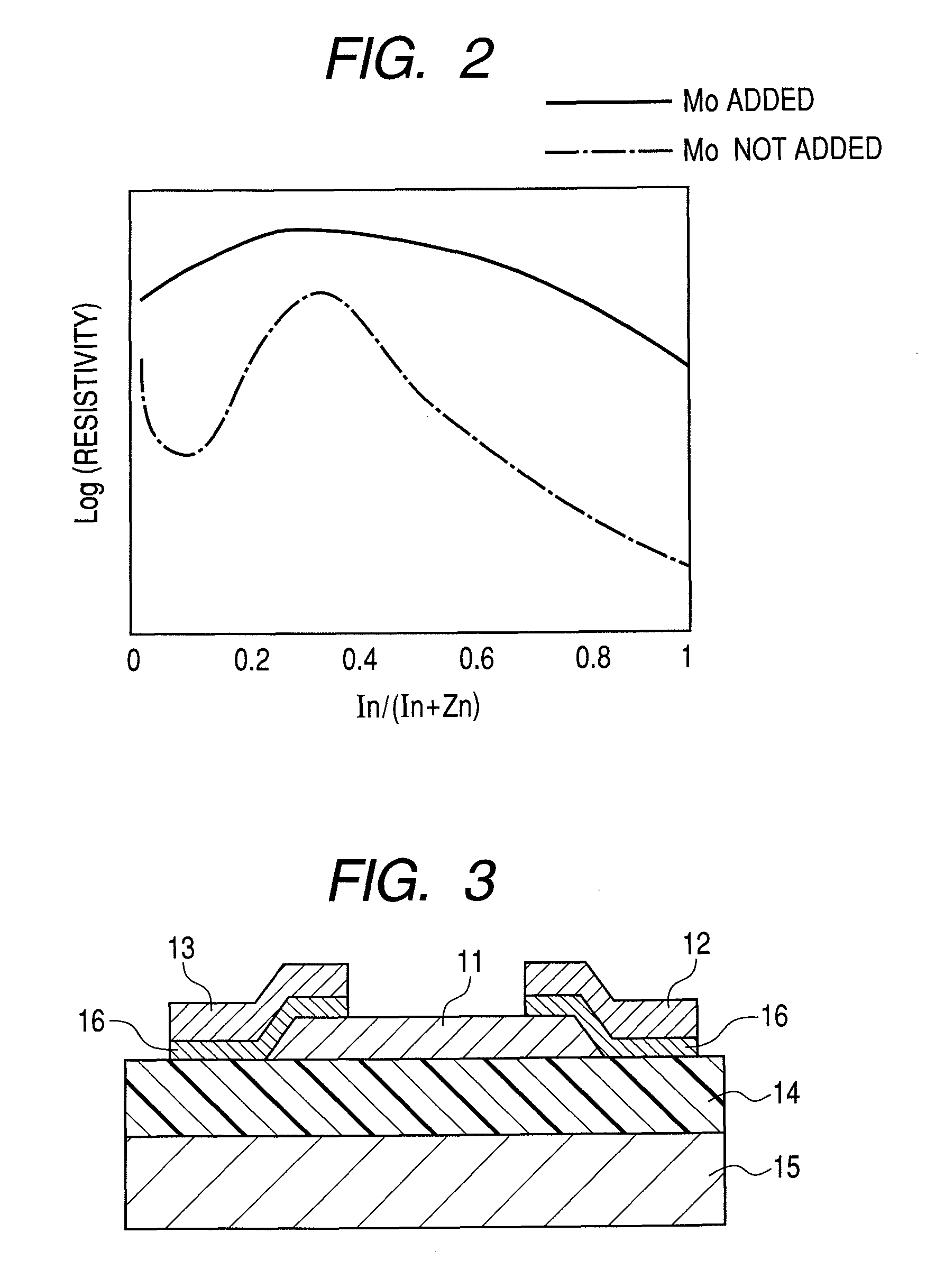
[0093]A second example of a TFT device according to the present invention is now described with reference to FIG. 4. In this example, an In—Zn—Ga—O film was used as the active layer.

[0094]In this example, Mo was used as the gate electrode 15 and a silicon oxide film at a thickness of about 150 nm was used as the gate insulating film 14. The substrate was a glass substrate, and the In—Zn—Ga—O film with Mo added thereto was formed on the glass substrate as the active layer 11.

[0095]The In—Zn—Ga—O film was formed using a co-sputtering apparatus with diagonal incidence configuration. In this example, there were three elements of In2O3, ZnO, and Ga2O3 in forming the film, and hence an In—Zn—Ga—O thin film having a Ga atomic composition ratio distribution of 1 atom % or higher and 10 atom % or lower in one substrate surface could be obtained. Further, here, a Ga concentration distribution was formed in a direction orthogonal to the composition slope of In—Zn.

[0096]As the target (material ...

example 3

[0113]A TFT device having the same structure as that of the above-mentioned Example 2 except for the electrodes was manufactured. In this example, an Mo electrode at a thickness of about 100 nm formed by an electron beam deposition method was used as the gate electrode 15, the source electrode 12, and the drain electrode 13.

[0114]In this example, the most satisfactory transistor characteristics were obtained when the atomic composition ratio of Ga, Ga / (In+Ga+Zn), was 1 atom % and when the atomic composition ratio of In expressed as In / (Zn+In) was about 30 to 80 atom %. In the range of the above-mentioned composition, independently of the atomic composition ratios of the metals, substantially similar characteristics were obtained. For example, the on-current Id was, when Vg=10 V, about 4×10⁻⁴ A, which was a larger value compared with the TFT in Example 2 in which the In—Zn—Ga—O film with Mo added thereto was used as the active layer. The reason is thought to be that, in this example,...


PUM

PropertyMeasurementUnit
electrical resistivityaaaaaaaaaa
humidityaaaaaaaaaa
temperatureaaaaaaaaaa

Abstract

An amorphous oxide at least includes: at least one element selected from the group consisting of In, Zn, and Sn; and Mo. An atomic composition ratio of Mo to a number of all metallic atoms in the amorphous oxide is 0.1 atom % or higher and 5 atom % or lower.

Description

TECHNICAL FIELD[0001]The present invention relates to an amorphous (also known as non-crystalline) oxide and a field effect transistor in which such an amorphous oxide is used for an active layer. The present invention also relates to a display apparatus in which organic EL or inorganic EL using such a transistor is used as a light-emitting device and to a display apparatus in which liquid crystal using such a transistor is used.BACKGROUND ART[0002]In recent years, semiconductor devices which use an amorphous-oxide-based semiconductor thin film have been receiving attention. Such a semiconductor thin film can be formed at low temperature, and has a large optical band gap and is optically transparent to visible light. Hence, a flexible transparent thin film transistor (TFT) or the like can be formed on a plastic substrate, a film substrate, or the like.[0003]As an example, Japanese Patent Application Laid-Open No. 2002-76356 discloses a technology with regard to a TFT in which an oxi...

Claims


Application Information

Patent Timeline
Patent Type & Authority Patents(United States)
IPC IPC(8): H01L29/10
CPCH01L29/7869
Inventor ITAGAKI, NAHOGOYAL, AMITAIWASAKI, TATSUYA
Owner CANON KK
Why Eureka
Try Eureka