Method of forming a layer on a semiconductor substrate and apparatus for performing the same

a technology of semiconductor substrate and underlying layer, which is applied in the direction of coating, chemical vapor deposition coating, metallic material coating process, etc., can solve the problems of affecting the performance difficult to adhere to other materials, and difficult to dry-etch copper, so as to improve the manufacturing throughput improve the characteristics of the thin layer of the semiconductor device, and prevent the underlying layer from deteriorating.

Inactive Publication Date: 2006-01-05
SAMSUNG ELECTRONICS CO LTD
View PDF5 Cites 344 Cited by
  • Summary
  • Abstract
  • Description
  • Claims
  • Application Information

AI Technical Summary

Benefits of technology

[0014] According to the present invention, the thin layer for a semiconductor device is formed through both an ALD process and a CVD process in the same chamber. The thin layer includes a first layer formed through the ALD process and a second layer formed through the CVD process. As a result, when a diffusion barrier layer or an upper electrode layer of a capacitor of a semiconductor device is formed as the thin layer of the present invention, a diffusion of impurities into an underlying layer is sufficiently prevented by the first layer formed through the ALD process, thereby preventing the deterioration of the underlying layer, the diffusion barrier layer and the upper electrode layer in a view of material characteristics. In addition, the second layer is formed through the CVD process, thereby improving a manufacturing throughput of a semiconductor device. Accordingly, the characteristics of the thin layer for a semiconductor device are remarkably improved with a superior manufacturing throughput and rare manufacturing failures.

Problems solved by technology

Whereas in the past aluminum (Al) has been the material of choice for such wiring due to its low specific resistance and ease of use in processing, extremely dense circuits owing to better manufacturing techniques require better conductor materials.
Unfortunately, copper has a major drawback in that copper atoms tend to diffuse into the silicon of the semiconductor substrate, thus affecting the performance of the semiconductor device.
Additionally, copper is more difficult to dry-etch than aluminum and is difficult to adhere to other materials, thereby presenting an uneven surface between the copper and a contiguous material.
However, titanium nitride (TiN) as a diffusion material creates several problems.
Most importantly, titanium nitride is difficult to apply to a semiconductor substrate.
Application of TiN via physical vapor deposition (PVD) often results in poor step coverage thus making such application method ill suited during highly integrated semiconductor devices.
Application of TiN via a chemical vapor deposition (CVD) process often results in diffusion of chloride ions (Cl−) from a base reactant gas into an underlying layer, thus resulting in degraded electrical characteristics of the resulting device.
Finally, application of TiN via an atomic layer deposition (ALD) is an extremely slow process thereby severely reducing manufacturing productivity.

Method used


Image

  • Method of forming a layer on a semiconductor substrate and apparatus for performing the same
  • Method of forming a layer on a semiconductor substrate and apparatus for performing the same
  • Method of forming a layer on a semiconductor substrate and apparatus for performing the same

Examples


first embodiment

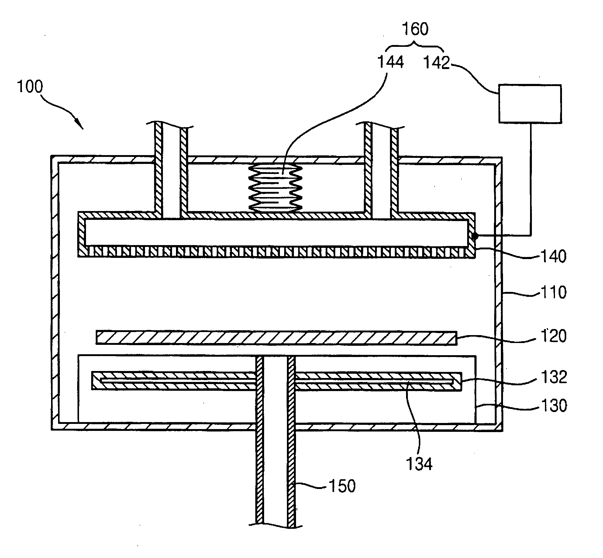
[0038]FIG. 2 is a cross sectional view illustrating an apparatus for forming a thin layer for a semiconductor device according to the present invention. FIGS. 3A and 3B are schematic views illustrating first and second layers of the thin layer formed on a substrate in the apparatus shown in FIG. 2.

[0039] Referring to FIG. 2, an apparatus 100 for forming a thin layer for a semiconductor device according to a first embodiment of the present invention includes a processing chamber 110 in which a semiconductor substrate 120 is positioned, a showerhead 140 through which reactants are provided into the processing chamber 110, an adjusting unit 160 for adjusting a gap distance between the showerhead 140 and the substrate 120, and a stage 130 for supporting the substrate 120. The showerhead 140 is positioned in an upper portion of the processing chamber 110, and the stage 130 is positioned in a lower portion of the processing chamber 110 and faces the showerhead 140.

[0040] In the present e...

second embodiment

[0051]FIG. 4 is a cross sectional view illustrating an apparatus for forming a thin layer for a semiconductor device according to the present invention. FIGS. 5A and 5B are schematic views illustrating first and second layers of the thin layer formed on a substrate in the apparatus shown in FIG. 4.

[0052] Referring to FIG. 4, an apparatus 200 for forming a thin layer for a semiconductor device according to a second embodiment of the present invention includes a processing chamber 210 in which a semiconductor substrate 220 is positioned, a showerhead 240 through which reactants are provided into the processing chamber 210, an adjusting unit 260 for adjusting a gap distance between the showerhead 240 and the substrate 220, and a stage 230 for supporting the substrate 220. The showerhead 240 is positioned in an upper portion of the processing chamber 210, and the stage 230 is positioned in a lower portion of the processing chamber 210 and faces the showerhead 240.

[0053] In the present ...

third embodiment

[0064]FIG. 6 is a cross sectional view illustrating an apparatus for forming a thin layer for a semiconductor device according to the present invention. FIGS. 7A and 7B are schematic views illustrating first and second layers of the thin layer formed on a substrate in the apparatus shown in FIG. 6.

[0065] Referring to FIG. 6, an apparatus 300 for forming a thin layer for a semiconductor device according to a third embodiment of the present invention includes a processing chamber 310 in which a semiconductor substrate 320 is positioned, a showerhead 340 through which reactants are provided into the processing chamber 310, first and second adjusting units 360 and 370 for adjusting a gap distance between the showerhead 340 and the substrate 320, and a stage 330 for supporting the substrate 320. The showerhead 340 is positioned in an upper portion of the processing chamber 310, and the stage 330 is positioned in a lower portion of the processing chamber 310 and faces the showerhead 340. ...


PUM

PropertyMeasurementUnit
temperatureaaaaaaaaaa
gap distanceaaaaaaaaaa

Abstract

In a method of forming a thin layer for a semiconductor device through an ALD process and a CVD process in the same chamber, a semiconductor substrate is introduced into a processing chamber, and an interval between a showerhead and the substrate is adjusted to a first gap distance. A first layer is formed on the substrate at a first temperature through an ALD process. The interval between the showerhead and the substrate is additionally adjusted to a second gap distance, and a second layer is formed on the first layer at a second temperature through a CVD process. Accordingly, the thin layer has good current characteristics, and the manufacturing throughput of a semiconductor device is improved.

Description

CROSS-REFERENCE OF RELATED APPLICATION [0001] This application relies for priority upon Korean Patent Application No. 2004-51855 filed on Jul. 5, 2004, the contents of which are herein incorporated by reference in their entirety. BACKGROUND OF THE INVENTION [0002] 1. Field of the Invention [0003] The present invention relates to a method of forming a layer on a semiconductor substrate and an apparatus for performing the same. More particularly, the present invention relates to a method of forming a layer using an atomic layer deposition (ALD) method followed by a chemical vapor deposition (CVD) method in the same processing chamber and an apparatus for performing the same. [0004] 2. Description of the Related Art [0005] Modern semiconductors use extremely small metal wiring. Whereas in the past aluminum (Al) has been the material of choice for such wiring due to its low specific resistance and ease of use in processing, extremely dense circuits owing to better manufacturing techniqu...

Claims


Application Information

Patent Timeline
Patent Type & Authority Applications(United States)
IPC IPC(8): C23C16/00
CPCC23C16/34C23C16/45589C23C16/45565C23C16/45544H01L21/205
Inventor SEO, JUNG-HUNPARK, YOUNG-WOOKHONG, JIN-GI
Owner SAMSUNG ELECTRONICS CO LTD
Why Eureka
Try Eureka