Gas distribution system for improved transient phase deposition

a gas distribution system and transient phase technology, applied in the field of semiconductor processing, can solve the problems of affecting certain desired properties of the resulting layer structure, poor adhesion between the oxide and the metal, and substantial difficulty in achieving a uniform liner, so as to ensure the quality of the deposition and good gapfill characteristics

Inactive Publication Date: 2006-06-01
APPLIED MATERIALS INC
View PDF20 Cites 347 Cited by
  • Summary
  • Abstract
  • Description
  • Claims
  • Application Information

AI Technical Summary

Benefits of technology

[0007] Embodiments of the present invention are directed to a gas distribution system which distributes the gas more uniformly into a process chamber during a transient phase when the gas initially flows via the gas distribution system into a process chamber. In specific embodiments, the gas distribution system incorporates variable orifice sizes between an outer channel and an inner channel. The gas flows via a gas inlet into the outer channel, and then travels through the orifices having different sizes into the inner channel. The size of an orifice increases with a distance between the orifi

Problems solved by technology

One issue that affects deposition properties in various such applications is diffusion between adjoining layers that have different compositions, which can adversely affect certain desired properties of the resulting layer structure.
For example, when doped silicon oxide is deposited in IMD applications, diffusion of the dopant to metal lines may cause the formation of und

Method used


Image

  • Gas distribution system for improved transient phase deposition
  • Gas distribution system for improved transient phase deposition
  • Gas distribution system for improved transient phase deposition

Examples


Embodiment Construction

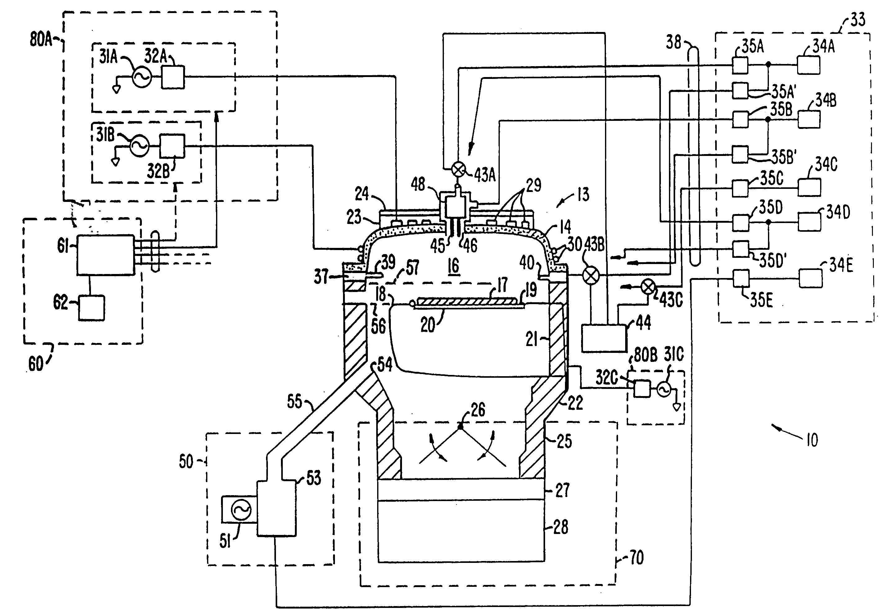
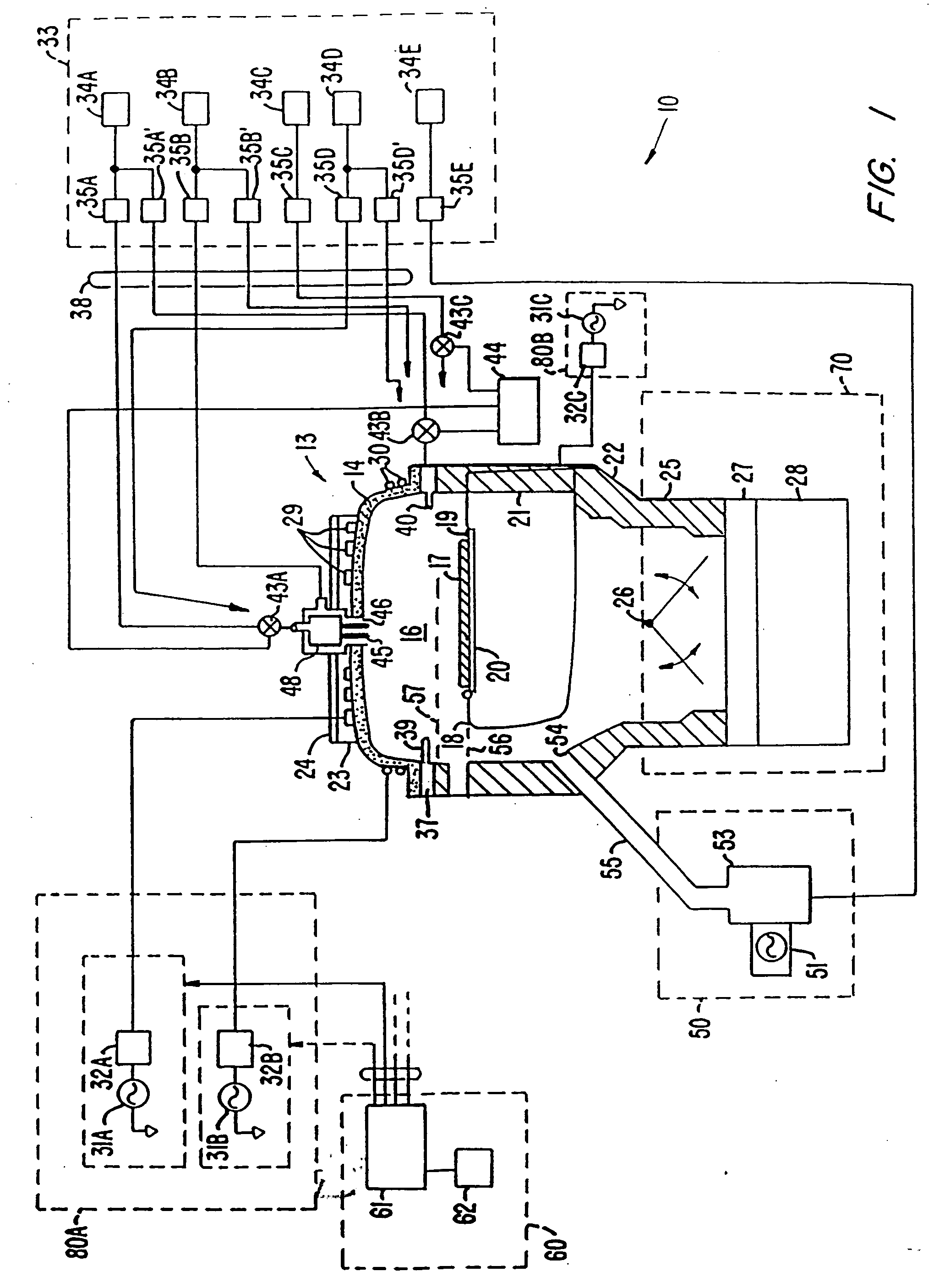
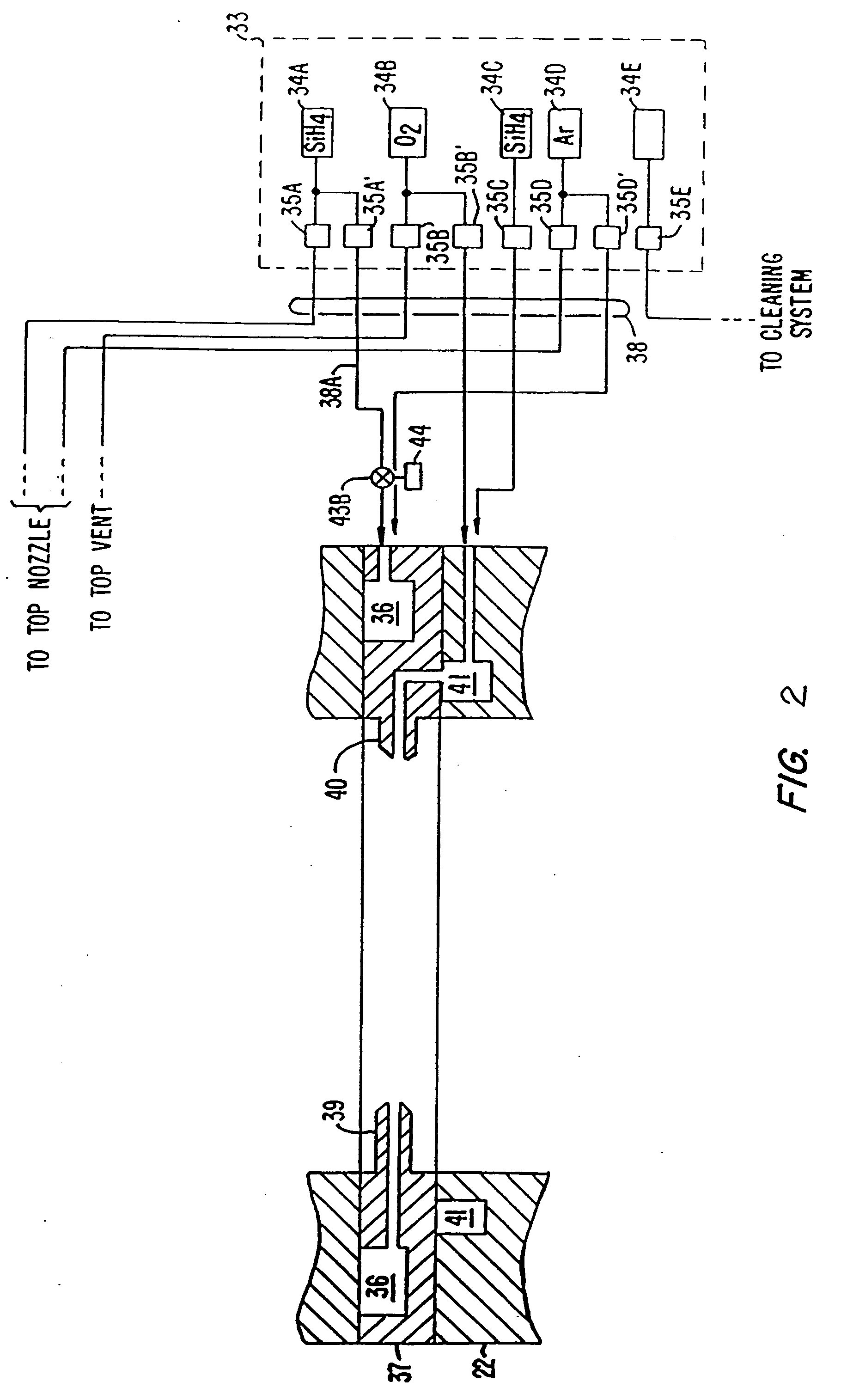
[0016]FIG. 1 illustrates one embodiment of a high density plasma chemical vapor deposition (HDP-CVD) system 10 in which a dielectric layer can be deposited. System 10 includes a chamber 13, a vacuum system 70, a source plasma system 80A, a bias plasma system 80B, a gas delivery system 33, and a remote plasma cleaning system 50.

[0017] The upper portion of chamber 13 includes a dome 14, which is made of a ceramic dielectric material, such as aluminum oxide or aluminum nitride. Dome 14 defines an upper boundary of a plasma processing region 16. Plasma processing region 16 is bounded on the bottom by the upper surface of a substrate 17 and a substrate support 18.

[0018] A heater plate 23 and a cold plate 24 surmount, and are thermally coupled to, dome 14. Heater plate 23 and cold plate 24 allow control of the dome temperature to within about ±10° C. over a range of about 100° C. to 200° C. This allows optimizing the dome temperature for the various processes. For example, it may be des...


PUM

PropertyMeasurementUnit
Angleaaaaaaaaaa
Sizeaaaaaaaaaa
Distanceaaaaaaaaaa

Abstract

Embodiments of the present invention are directed to a gas distribution system which distributes the gas more uniformly into a process chamber. In one embodiment, a gas distribution system comprises a gas ring including an outer surface and an inner surface, and a gas inlet disposed at the outer surface of the gas ring. The gas inlet is fluidicly coupled with a first channel which is disposed between the outer surface and the inner surface of the gas ring. A plurality of gas outlets are distributed over the inner surface of the gas ring, and are fluidicly coupled with a second channel which is disposed between the outer surface and the inner surface of the gas ring. A plurality of orifices are fluidicly coupled between the first channel and the second channel. The plurality of orifices are spaced from the gas inlet by a plurality of distances, and have sizes which vary with the distances from the gas inlet as measured along the first channel, such that the size of the orifice increases with an increase in the distance between the orifice and the gas inlet as measured along the first channel.

Description

CROSS-REFERENCES TO RELATED APPLICATIONS [0001] This application claims the benefit of U.S. Provisional Patent Application No. 60 / 631,714, filed Nov. 29, 2004, the entire disclosure of which is incorporated herein by reference.BACKGROUND OF THE INVENTION [0002] This invention relates generally to semiconductor processing and, more particularly, to an improved gas distribution system, for instance, for a chemical vapor deposition chamber to provide improved transient phase deposition. [0003] One of the primary steps in the fabrication of modem semiconductor devices is the formation of a thin layer on a semiconductor substrate by chemical reaction of gases. Such a deposition process is referred to generally as chemical-vapor deposition (“CVD”). Conventional thermal CVD processes supply reactive gases to the substrate surface where heat-induced chemical reactions take place to produce a desired layer. Plasma-enhanced CVD (“PECVD”) techniques, on the other hand, promote excitation and / o...

Claims


Application Information

Patent Timeline
IPC IPC(8): H01L21/306C23F1/00
CPCC23C16/4558C23C16/00C23C16/455
Inventor GONDHALEKAR, SUDHIRDUNCAN, ROBERTSALIMIAN, SIAMAKRASHEED, MUHAMMAD M.WHITESELL, HARRY SMITHGEOFFRION, BRUNOKRISHNARAJ, PADMANABHANGUJER, RUDOLF
Owner APPLIED MATERIALS INC
Why Eureka
Try Eureka