

Method of forming a carbon polymer film using plasma CVD
a carbon polymer and plasma cvd technology, applied in the direction of liquid surface applicators, instruments, coatings, etc., can solve the problem of difficult formation of thin films on substrates, and achieve the effect of excellent characteristics and high functionality
- Summary
- Abstract
- Description
- Claims
- Application Information
AI Technical Summary
Benefits of technology
Problems solved by technology
Method used
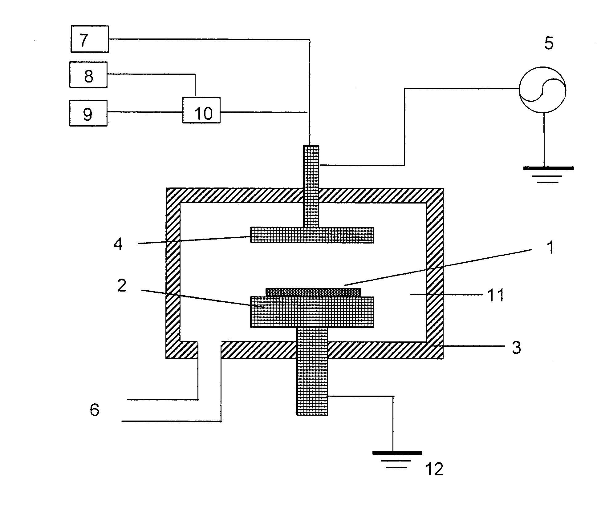
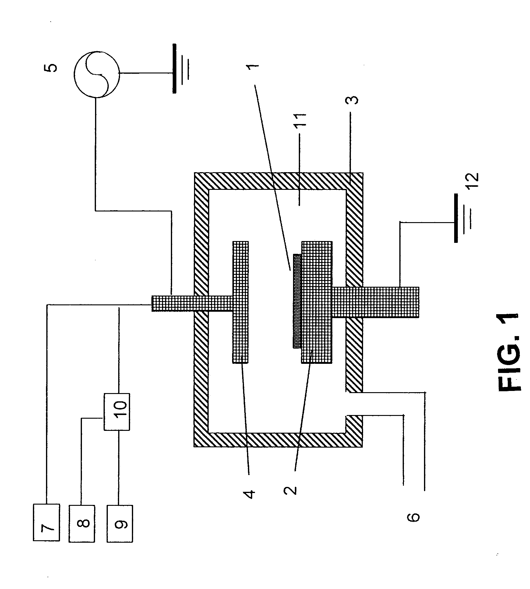
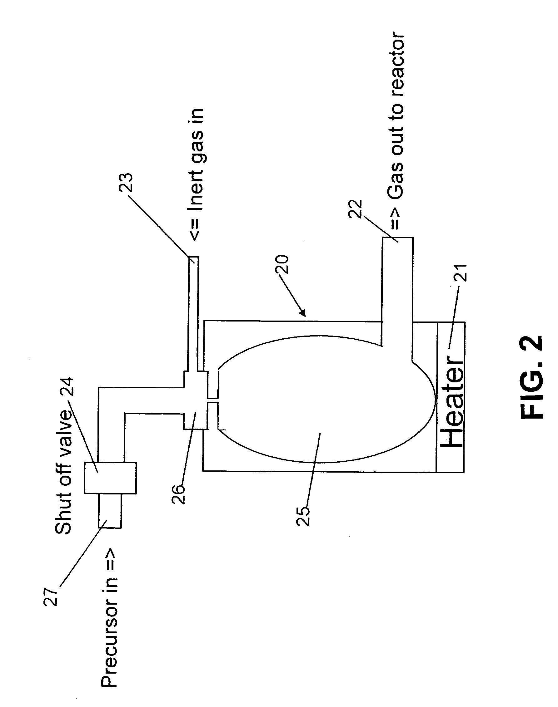
Image

Examples
example 1
Process Conditions in this Example and Film Formation Results are Shown as Follows
[0097] Gap between shower plate and susceptor: 12 mm
[0098] Process Conditions:
[0099] TMB (1,3,5-trimethyl-benzene, C6H5(CH3)3): 70 sccm
[0100] He supplied to vaporizer: 50 sccm
[0101] Process gas He supplied to reactor: 50 sccm
[0102] Ar: 50 sccm
[0103] RF Power 27 MHz: 1400 W
[0104] Pressure: 270 Pa
[0105] Film formation time: 70 sec
[0106] Film Formation Results:
[0107] Thickness: 200 nm
[0108] RI(n): 1.67
[0109] RI(k): 0.02 @633 nm
[0110] Modulus: 7 GPa
[0111] Hardness: 0.7 GPa
[0112] (Controllability of Thin Film Formation)
[0113] Additionally, FIG. 3 shows relation of film formation time and a thickness of a film formed obtained under the same conditions as the above. A film thickness is proportional to the film formation time; it was confirmed that thin films having a thickness from approximately 30 nm to approximately 400 nm were formed with satisfactory controllability. Additionally, RI, mod...
example 2
Process Conditions in this Example and Film Formation Results are Shown as Follows
[0114] Gap between shower plate and susceptor: 12 mm
[0115] Process Conditions:
[0116] TMB: 70 sccm
[0117] He supplied to vaporizer: 50 sccm
[0118] Process gas He supplied to reactor: 50 sccm
[0119] Ar: 50 sccm
[0120] RF Power 27 MHz: 1400 W
[0121] Pressure: 270 Pa
[0122] Film formation time: 18 sec
[0123] Film Formation Results:
[0124] Thickness: 50 nm
[0125] RI(n): 1.67
[0126] RI(k): 0.02 @633 nm
[0127] Modulus: 7 GPa
[0128] Hardness: 0.7 GPa
example 3
Process Conditions in this Example and Film Formation Results are Shown as Follows
[0129] Gap between shower plate and susceptor: 24 mm
[0130] Process Conditions:
[0131] TMB: 280 sccm
[0132] He supplied to vaporizer: 50 sccm
[0133] Process gas He supplied to reactor: 50 sccm
[0134] Ar: 50 sccm
[0135] RF Power 27 MHz: 1400 W
[0136] Pressure: 270 Pa
[0137] Film formation time: 430 sec
[0138] Film Formation Results:
[0139] Thickness: 245 nm
[0140] RI(n): 1.82
[0141] RI(k): 0.015 @633 nm
[0142] Modulus: 5.6 GPa
[0143] Hardness: 0.4 GPa
PUM
 Abstract
Description
Claims
Application Information