Method for repairing damage of dielectric film by cyclic processes

a dielectric film and process technology, applied in the direction of coatings, chemical vapor deposition coatings, metallic material coating processes, etc., can solve the problems of increasing dielectric constants and/or leakage currents, physical damage caused by chemical mechanical planarization (cmp), and increasing dielectric constants.

Active Publication Date: 2014-07-22
ASM IP HLDG BV
View PDF9 Cites 382 Cited by
  • Summary
  • Abstract
  • Description
  • Claims
  • Application Information

AI Technical Summary

Benefits of technology

[0013]In some embodiments, steps (ii) and (iii) correspond to a pore-sealing step of the surface-restored dielectric film, wherein pores on the surface are sealed with a pore-sealing film formed using the second gas (which may also be referred to as a “pore-sealing gas”). In some embodiments, the pore-sealing film is constituted by a SiCN material and is capable of completely inhibiting chemical diffusion and significantly improving a barrier function (e.g., resistance to O2 plasma), and is formed by plasma-enhanced atomic layer deposition (PEALD) at a relatively low temperature (e.g., about 150° C. to about 400° C.), thereby forming a film having good characteristics. Since RF power is not exerted directly on the second gas, but is exerted on a reactant, no oxygen radicals nor ammonia radicals are generated from the second gas, thereby sealing pores by a pore-sealing film without significantly causing further damage by radicals to the surface of the dielectric film. In some embodiments, the pulse of the second gas per cycle is about 0.1 seconds to about 10 seconds (preferably about 0.3 seconds to about 3 seconds), which is shorter than the duration of the first gas supply. Since the pore-sealing film is intended to be deposited mainly on a top surface, the pulse of the second gas can be shorter than the duration of the first gas supply. In some embodiments, some pores may be closed by the pore-sealing film while leaving voids in other pores. In some embodiments, the number of cycles for depositing a pore-sealing film is 10 to 1,000, typically 20 to 400.

Problems solved by technology

Dielectric films are susceptible to damage during their manufacturing processes, thereby increasing dielectric constants and / or leakage currents.
Such process-related damage includes damage caused by dry etching and plasma ashing, and washing with chemicals, and physical damage by chemical mechanical planarization (CMP), etc.
Such porous low-k films are highly susceptible to damage during an etching process for patterning or the like, and when the films are damaged, the dielectric constant values increase.
However, although damaged surfaces can be restored to a certain degree by the above methods using a hydrocarbon film, restoration is insufficient depending on the degree of damage.
Further, a hydrocarbon film can seal pores of the damaged surfaces, but the hydrocarbon film does not have sufficient barrier function as a pore-sealing film against a barrier metal although it can inhibit diffusion of chemicals such as toluene to a certain degree.
In some embodiments, although in steps (ii) and (iii), the pore-sealing film is deposited by atomic layer deposition, the surface of the dielectric film is exposed to radicals until the pores are sealed and thus is subject to damage by radicals.

Method used


Image

  • Method for repairing damage of dielectric film by cyclic processes
  • Method for repairing damage of dielectric film by cyclic processes
  • Method for repairing damage of dielectric film by cyclic processes

Examples


example 1

[0072]1) A Si substrate (300 mm in diameter) was placed in the reactor and a siloxane polymer film was formed on the substrate using Aurora® X (diethoxymethylsilane; ASM International N.V.) and Pore Builder™ (hydrocarbon for atom transfer radical polymerization; ASM International N.V.), He, and O2. The substrate with the siloxane polymer film was transferred to a UV reactor and subjected to UV cure, thereby obtaining an ELK film having a dielectric constant of 2.00, a porosity of 40%, and a thickness of 200 nm.

[0073]2) Next, the substrate with the ELK film was transferred to a reactor for plasma ashing or etching under the conditions shown in Table 7 below, thereby causing plasma damage to the ELK film. As a result of the plasma damage, the dielectric constant of the ELK film increased to 2.42.

[0074]

TABLE 7Damage conditionRF frequency (MHz)13.56 MHzHRF (W)60 WTreatment time (sec)24 secSubstrate temperature (° C.)250°C.Pressure (Pa)466 PaHe (sccm)2000 sccmO2 (sccm)12 sccmGAP (mm)8 mm...

example 2

[0079]In a manner substantially similar to that in Example 1, a damaged ELK film was prepared, which had a dielectric constant of 2.40. The damaged ELK was subjected to the restoration step and the pore-sealing cycles in the same manner as in Example 1 to obtain a pore-sealed ELK film. Next, the pore-sealed ELK film was loaded into the reactor and exposed to an oxygen plasma (an O2 flow of 12 sccm, RF power of 60 W, a duration of 24 sec, a pressure of 5 Torr, a temperature of 250° C.). The dielectric constant of the plasma-exposed ELK film was 2.40, which was unchanged from that before the oxygen plasma exposure, indicating that the pore-sealing significantly improved resistance to an oxygen plasma, which is indicative of resistance to diffusion of a metal.

examples 3 and 4

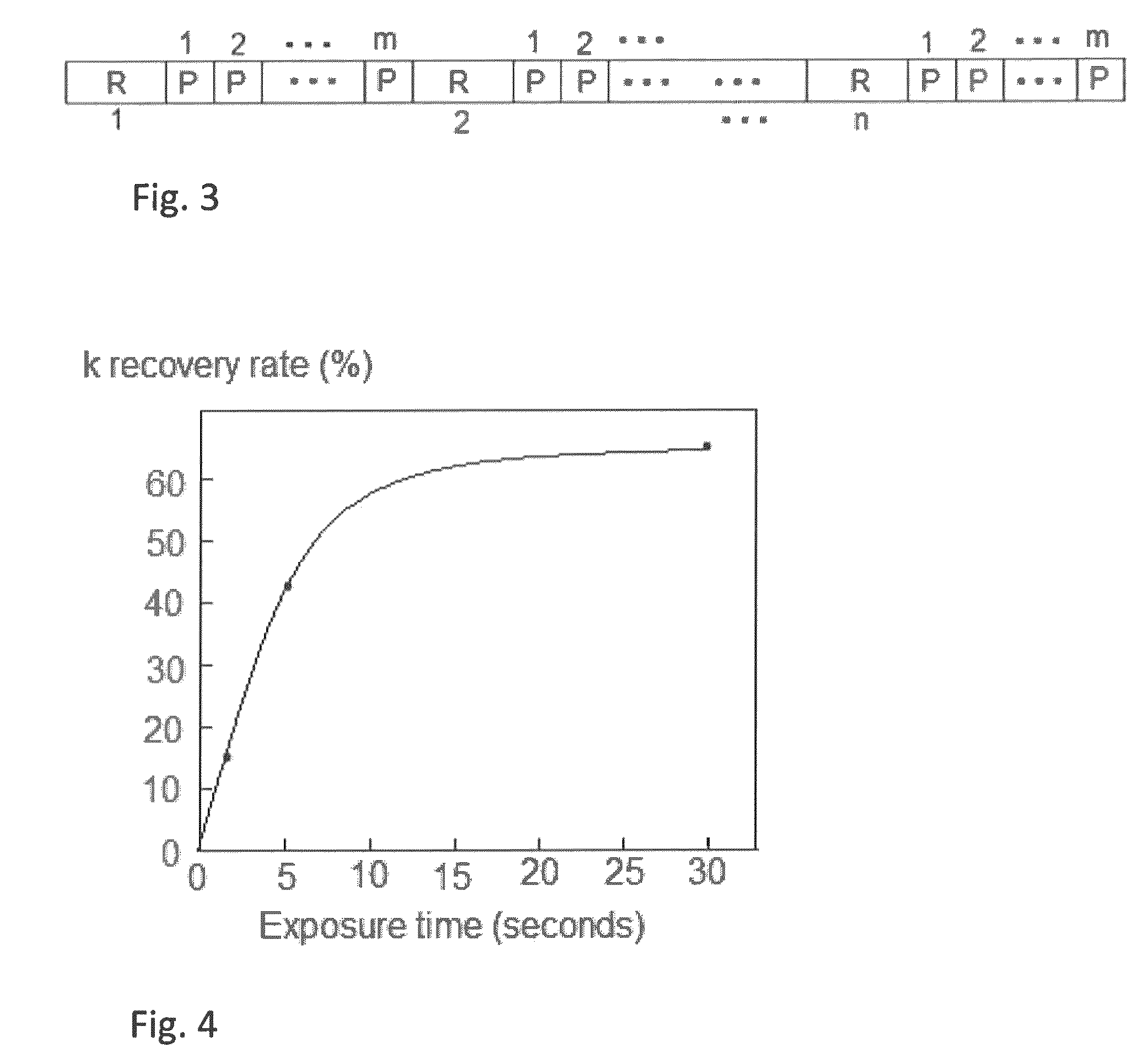
[0081]In a manner substantially similar to that in Example 1, an ELK film was prepared and then subjected to plasma damage to obtain a damaged ELK film. The damaged ELK was subjected to the restoration step in the same manner as in Example 1 except for the duration of gas exposure to obtain a surface-restored ELK film. The duration of gas exposure was 1.5 seconds (Example 3) and 5 seconds (Example 4) as compared with 30 seconds (Example 1). The dielectric constant of each film is shown in Table 10 below. As shown in Table 10, when the duration of gas exposure was 5 seconds, the dielectric constant decreased from 2.45 to 2.26, i.e., the recovery rate [(2.45−2.26) / (2.45−2.00)] was 42% (Example 3), and when the duration of gas exposure was 1.5 seconds, the dielectric constant decreased from 2.43 to 2.36, i.e., the recovery rate [(2.43−2.36) / (2.43−2.00)] was 16% (Example 4). In Example 1, when the duration of gas exposure was 30 seconds, the dielectric constant decreased from 2.42 to 2....


PUM

PropertyMeasurementUnit
thicknessaaaaaaaaaa
dielectric constantaaaaaaaaaa
temperatureaaaaaaaaaa

Abstract

A method for repairing process-related damage of a dielectric film includes: (i) adsorbing a first gas containing silicon on a surface of the damaged dielectric film without depositing a film in the absence of reactive species, (ii) adsorbing a second gas containing silicon on a surface of the dielectric film, followed by applying reactive species to the surface of the dielectric film, to form a monolayer film thereon, and (iii) repeating step (ii). The duration of exposing the surface to the first gas in step (i) is longer than the duration of exposing the surface to the second gas in step (ii).

Description

CROSS-REFERENCE TO RELATED APPLICATIONS[0001]This application claims the benefit of U.S. Provisional Application No. 61 / 653,969, filed May 31, 2012 under 35 USC 119(e), the disclosure of which is herein incorporated by reference in its entirety.BACKGROUND[0002]1. Field of the Invention[0003]The present invention generally relates to a method for repairing process-related damage of a dielectric film by cyclic processes.[0004]2. Description of the Related Art[0005]Dielectric films are indispensable to increasing processing speed of semiconductor devices and lowering power consumption of the devices. Dielectric films are susceptible to damage during their manufacturing processes, thereby increasing dielectric constants and / or leakage currents. Such process-related damage includes damage caused by dry etching and plasma ashing, and washing with chemicals, and physical damage by chemical mechanical planarization (CMP), etc. Particularly, in advanced devices, dielectric films are porous a...

Claims


Application Information

Patent Timeline
Patent Type & Authority Patents(United States)
IPC IPC(8): H01L21/00H01L21/768
CPCH01L21/76825C23C16/045C23C16/45527H01L21/02167H01L21/02274H01L21/0228H01L21/3105H01L21/76814H01L21/76826H01L21/76831
Inventor KOBAYASHI, AKIKOKIMURA, YOSUKEISHIKAWA, DAIMATSUSHITA, KIYOHIRO
Owner ASM IP HLDG BV
Why Eureka
Try Eureka