Process for the production of thin semiconductor material films

a technology of semiconductor material and production process, which is applied in the direction of stone-like material working apparatus, instruments, electrical apparatus, etc., can solve the problems of difficult production of monocrystalline films, difficult to produce monocrystalline films, and disadvantages of production procedures for producing thin monocrystalline films, etc., and achieve uniform and controlled thickness

Inactive Publication Date: 2007-02-06
COMMISSARIAT A LENERGIE ATOMIQUE ET AUX ENERGIES ALTERNATIVES
View PDF69 Cites 306 Cited by
  • Summary
  • Abstract
  • Description
  • Claims
  • Application Information

AI Technical Summary

Benefits of technology

[0012]The present invention relates to a process for producing thin semiconductor material films making it possible to overcome the aforementioned disadvantages without requiring an initial substrate of a ...

Problems solved by technology

It is known that for producing monocrystalline semiconductor films there are various methods and processes, which are often complex and expensive to carry out, because although it is relatively easy to produce polycrystalline or amorphous material films, it is much more difficult to produce monocrystalline films.
The various methods for producing thin monocrystalline films suffer from the disadvantages associated with the production procedures.
Heteroepitaxy methods are limited by the nature of the substrate, because the lattice parameter of the substrate is not precisely the same as that of the ...

Method used


Image

  • Process for the production of thin semiconductor material films
  • Process for the production of thin semiconductor material films

Examples


Embodiment Construction

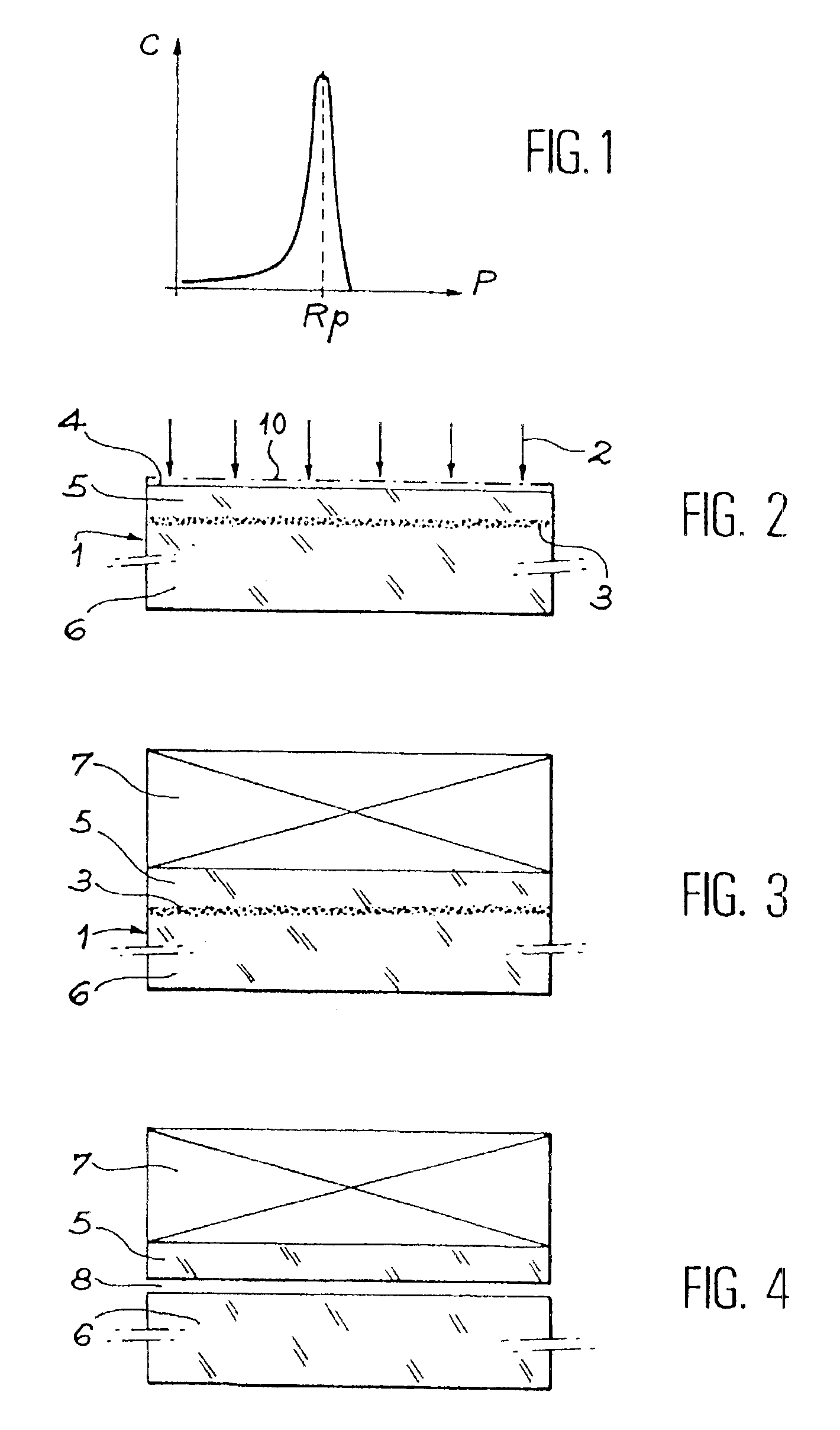
[0033]The embodiment which will now be described in conjunction with the above drawings relates to the production of a thin film in a monocrystalline silicon wafer with the aid of H+ ion implantations.

[0034]The implantation of H+ ions (protons) at 150 keV in a monocrystalline silicon wafer, whose surface corresponds to a principle crystallographic plane, e.g. a 1,0,0 plane lead, in the case of weak implantation doses (16 cm−2) to a hydrogen concentration profile C as a function of the depth P having a concentration maximum for a depth Rp, as shown in FIG. 1. In the case of a proton implantation in silicon, Rp is approximately 1.25 micrometers.

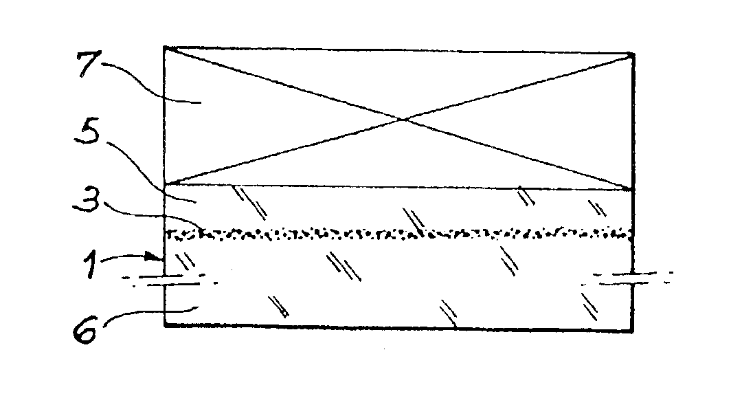
[0035]For doses of approximately 1016 cm−2, the implanted hydrogen atoms start to form bubbles, which are distributed in the vicinity of a plane parallel to the surface. The plane of the surface corresponds to a principal crystallographic plane and the same applies with respect to the plane of the microbubbles, which is consequently a cleaving ...


PUM

PropertyMeasurementUnit
Temperatureaaaaaaaaaa
Angleaaaaaaaaaa

Abstract

Process for the preparation of thin monocrystalline or polycrystalline semiconductor material films, characterized in that it comprises subjecting a semiconductor material wafer having a planar face to the three following stages: a first stage of implantation by bombardment (2) of the face (4) of the said wafer (1) by means of ions creating in the volume of said wafer a layer (3) of gaseous microbubbles defining in the volume of said wafer a lower region (6) constituting the mass of the substrate and an upper region (5) constituting the thin film, a second stage of intimately contacting the planar face (4) of said wafer with a stiffener (7) constituted by at least one rigid material layer, a third stage of heat treating the assembly of said wafer (1) and said stiffener (7) at a temperature above that at which the ion bombardment (2) was carried out and sufficient to create by a crystalline rearrangement effect in said wafer (1) and a pressure effect in the said microbubbles, a separation between the thin film (5) and the mass of the substrate (6).

Description

BACKGROUND OF THE INVENTION[0001]The present invention relates to a process for the production of thin semiconductor material films, preferably applicable to the production of monocrystalline films.[0002]It is known that for producing monocrystalline semiconductor films there are various methods and processes, which are often complex and expensive to carry out, because although it is relatively easy to produce polycrystalline or amorphous material films, it is much more difficult to produce monocrystalline films.[0003]Among the methods used for producing monocrystalline films are those used for producing socalled “silicon on insulator” substrates, where the aim is to produce a monocrystalline silicon film resting on a substrate electrically insulated from the film.[0004]By crystal growth heteroepitaxy methods make it possible to grow an e.g. thin film silicon crystal on a monocrystalline substrate of another type, whose lattice parameter is close to that of silicon, e.g. a sapphire ...

Claims


Application Information

Patent Timeline
IPC IPC(8): H01L21/42H01L21/324H01L21/477H01L29/12H01L21/205B28D1/00B28D5/00G01L9/00H01L21/02H01L21/027H01L21/265H01L21/762H01L27/12H01L31/04H01L33/00
CPCB28D1/005B28D5/00G01L9/0042H01L21/26506H01L21/76243H01L2221/68363Y10S148/012H01L33/0093H01L21/185H01L21/76254
Inventor BRUEL, MICHEL
Owner COMMISSARIAT A LENERGIE ATOMIQUE ET AUX ENERGIES ALTERNATIVES
Why Eureka
Try Eureka