Semiconductor process equipment

A process equipment and semiconductor technology, applied in semiconductor/solid-state device manufacturing, discharge tubes, electrical components, etc., can solve the problem of reducing the passage rate of free radicals, affecting the chemical reaction effect of free radicals and the surface of wafer 1-5, and reducing the passage of ions rate and other issues

Pending Publication Date: 2022-02-22
BEIJING NAURA MICROELECTRONICS EQUIP CO LTD
View PDF14 Cites 0 Cited by
  • Summary
  • Abstract
  • Description
  • Claims
  • Application Information

AI Technical Summary

Problems solved by technology

[0007] However, in order to ensure the filtering effect of ions in the plasma and prevent parasitic discharges in the through holes, it is necessary to reduce the aperture of the through holes to the level of the width of the plasma sheath (usually below the millimeter level), which is extremely difficult to process
In addition, reducing the aperture of the through hole will reduce the passage rate of free radicals in the plasma in almost the same proportion while reducing the passage rate of ions in the plasma (for example, the filtration ratio of the filter structure for ions and free radicals is close to 1: 1), thereby affecting the chemical reaction effect of free radicals and the surface of wafer 1-5, which is not conducive to the pre-cleaning effect of wafer 1-5

Method used


Image

  • Semiconductor process equipment
  • Semiconductor process equipment
  • Semiconductor process equipment

Examples


Embodiment 1

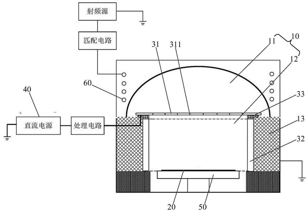
[0043] Such as figure 2 As shown, in Embodiment 1, the filter structure further includes a first extension 32, and the first extension 32 is along the axial direction of the process chamber 10 (that is, the vertical direction of the process chamber 10 shown in the figure, which can also be considered as The approximate moving direction of the plasma) extends and circles around the process chamber 10 , that is to say, the first extension portion 32 is approximately cylindrical. The first extension part 32 is entirely made of conductive material. The first extension portion 32 is in contact with the circumferential cavity wall 13 of the process cavity 10 (that is, the circumferential cavity wall of the processing cavity 12 ). Since the circumferential cavity wall 13 of the process chamber 10 is always grounded, the first extension portion 32 is grounded by being in contact with the circumferential cavity wall 13 .

[0044] Normally, the first extension portion 32 is relativel...

Embodiment 2

[0052] Such as Figure 4 As shown, in Embodiment 2, the filter structure further includes a second extension 34, and the second extension 34 is along the axial direction of the process chamber 10 (that is, the vertical direction of the process chamber 10 shown in the figure, which can also be considered as The approximate moving direction of the plasma) extends and circles around the process chamber 10 , that is to say, the second extension portion 34 is approximately cylindrical. The second extension part 34 is entirely made of conductive material. The first filter part 31 is integrally connected with the top end of the second extension part 34 . That is to say, the DC power supply 40 applies a negative voltage to the first filter part 31 and the second extension part 34 at the same time. Normally, the second extension part 34 should be relatively fixed to the circumferential chamber wall 13 of the process chamber 10 , so that the first filter part 31 can be effectively sup...

Embodiment 3

[0061] Such as Figure 5 As shown, in the third embodiment, the filter structure further includes a third extension 37, the third extension 37 extends along the axial direction of the process chamber 10 and circles around the circumference of the process chamber 10, that is to say, the third extension The portion 37 is substantially cylindrical. The third extension 37 is made of conductive material. The second filter part 36 is integrally connected with the top end of the third extension part 37 . The third extension portion 37 is in contact with the circumferential chamber wall 13 of the process chamber 10 . Since the circumferential cavity wall 13 of the process chamber 10 is always grounded, the second filter part 36 and the third extension part 37 are grounded by being in contact with the circumferential cavity wall 13 as a whole.

[0062] The filtering structure further includes a third insulating part 38 , the first filtering part 31 is connected and fixed to the thir...


PUM


Abstract

The invention provides semiconductor process equipment, and the equipment comprises a process chamber provided with a process cavity, wherein the process cavity comprises a generation cavity for generating plasma and a processing cavity for processing a wafer; a filtering structure and a direct-current power supply, wherein the filtering structure comprises a first filtering part, the first filtering part is arranged between the generating cavity and the processing cavity, is provided with a plurality of first through holes for communicating the generating cavity with the processing cavity, and is made of a conductive material, and the direct-current power supply is electrically connected with the first filtering part, and a negative voltage is applied to the first filtering part through the direct-current power supply; when the plasma passes through the first filtering part, the plasma is filtered through the multiple first through holes, and at least part of ions in the plasma are compounded under the action of the negative voltage, so that the number of ions in the plasma entering the processing cavity after filtering is reduced. According to the invention, the influence on the number of free radicals entering the processing cavity can be reduced as much as possible while the number of ions entering the processing cavity is reduced.

Description

technical field [0001] The present invention relates to the technical field of semiconductor process, and in particular, to a semiconductor process equipment. Background technique [0002] In the semiconductor process flow, before the coating process on the wafer, it is generally necessary to perform pre-cleaning treatment to remove impurities (such as oxides, organic substances, etc.) on the wafer surface, increase the cleanliness of the wafer surface or perform Molecular-level activation, thereby improving the adhesion of deposited films in subsequent coating processes (such as physical vapor deposition processes), improving process reliability and product yield. [0003] The basic principle of the pre-cleaning treatment is to bombard the surface of the wafer with ions in the plasma and / or to react with the surface of the wafer through free radicals in the plasma, so as to remove impurities. A process gas (eg, argon, hydrogen, helium, etc.) is ignited into a plasma within...

Claims


Application Information

Patent Timeline
Patent Type & Authority Applications(China)
IPC IPC(8): H01J37/32H01L21/67B08B7/00B08B13/00
CPCH01J37/32082H01J37/32357H01J37/32422H01L21/67028B08B7/00B08B13/00
Inventor 魏延宝苏振宁朱旭
Owner BEIJING NAURA MICROELECTRONICS EQUIP CO LTD
Why Eureka
Try Eureka