Ion implantation apparatus

An ion implantation device and ion implantation technology are applied in discharge tubes, electrical components, circuits, etc., and can solve problems such as difficulty in single ion implantation

Active Publication Date: 2015-10-28
PARCAN NANOTECH CO LTD
View PDF4 Cites 1 Cited by
  • Summary
  • Abstract
  • Description
  • Claims
  • Application Information

AI Technical Summary

Problems solved by technology

However, it is still very difficult to achieve single ion implantation, and how to improve single ion implantation technology has become an urgent technical demand

Method used


Image

  • Ion implantation apparatus
  • Ion implantation apparatus
  • Ion implantation apparatus

Examples


Embodiment 1

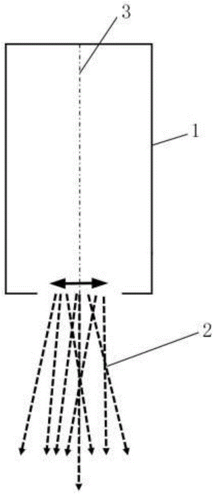
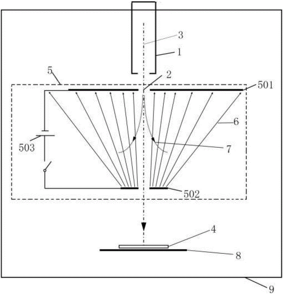
[0042] This embodiment provides an ion implantation device for implanting ions into a sample 4, such as figure 2 As shown, it includes: an ion source 1, which is used to generate and emit an ion beam 2; and a first electrode device 5, which is arranged on the path from the ion source 1 to the sample 4, and is used to generate ion beams along the The cone-shaped electric field 6 distributed in the direction of the central axis of the source, and the ions in the ion beam 2 that do not move along the direction of the central axis 3 are deflected in the direction perpendicular to the central axis 3 under the action of the cone-shaped electric field 6 and are not injected. the sample.

[0043]In this embodiment, the first electrode device 5 includes: an upper electrode plate 501 with a small hole, which is arranged on the path from the ion source 1 to the sample 4, and close to the ion source 1; There is a lower electrode plate 502 with a small hole, which is arranged on the path...

Embodiment 2

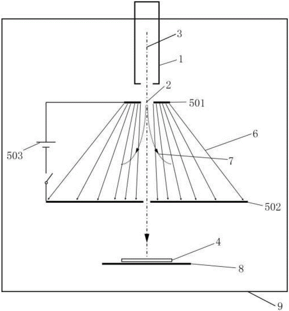
[0050] Compared to Example 1, such as image 3 As shown, the size of the lower electrode plate 502 in this embodiment is larger than that of the upper plate electrode 501, and the current direction of the first bias power supply is changed accordingly, so that the direction of the electric field lines of the conical electric field formed is opposite to that of the first embodiment. Through this conical electric field, the effect of diluting the ion beam can also be achieved.

Embodiment 3

[0052] Compared to Example 1, such as Figure 4 As shown, the upper electrode plate 501 and the lower electrode plate 502 in this embodiment are curved electrode plates with different sizes, and a conical electric field along the central axis direction of the ion source is formed by these two curved electrode plates. And through the conical electric field, the effect of diluting the ion beam can also be achieved.


PUM


Abstract

The invention relates to the field of electronic devices, and discloses an ion implantation apparatus. The ion implantation apparatus comprises an ion source used for generating and emitting ion beams and a first electrode device arranged on a path from the ion source to a sample, the first electrode device is used for generating a tapered electric field distributed along the direction of the central axis of the ion source and enabling ions which do not move along the direction of the central axis of the ion source in the ion beams to deflect along the direction vertical to the central axis and not to be implanted into the sample under the effect of the tapered electric field, a second electrode device is arranged at the downstream position of the first electrode device and used for generating an electric field for assisting the ions to deflect, when the electric field is applied, the ions along the direction of the central axis deflect and are not implanted into the sample, and when the electric filed is not applied, the ions along the direction of the central axis penetrate through the second electrode device and are implanted into the sample. According to the ion implantation apparatus, the dilution of the ion beams is performed via the tapered electric field, an ion gate is formed via the transverse electric field, and the implantation of a few ions or even a single ion is realized.

Description

technical field [0001] The invention relates to the field of electronic devices, in particular to an ion implantation device. Background technique [0002] With the further improvement of the integration level of integrated circuits, the size of microelectronic devices is further reduced from micron to nanometer, even to several nanometers. Subsequently, the relevant technologies and processes for making devices must also change, and ion implantation is one of the key technologies. It is well known in the art that only a limited number of ions implanted with a specific spatial distribution in the tiny nanometer dimensions of a device can form reasonable characteristics of the device. The implantation of a small amount of ions, or even a few ions, cannot be achieved by pure field emission technology, so it is necessary to consider the single ion implantation technology that only implants a few or even a single ion at a time. However, it is still very difficult to achieve si...

Claims


Application Information

Patent Timeline
Patent Type & Authority Applications(China)
IPC IPC(8): H01J37/317H01J37/30
Inventor 周向前瞿鑫
Owner PARCAN NANOTECH CO LTD
Why Eureka
Try Eureka