Method of forming semiconductor device

A semiconductor and device technology, applied in the field of semiconductor device formation, can solve problems such as poor semiconductor structure performance, achieve the effect of reducing the number of ions and improving adjustment accuracy

Active Publication Date: 2018-06-01
SEMICON MFG INT (SHANGHAI) CORP
View PDF4 Cites 0 Cited by
  • Summary
  • Abstract
  • Description
  • Claims
  • Application Information

AI Technical Summary

Problems solved by technology

[0017] The problem solved by the present invention is that the performance of the semiconductor structure formed by the method of the prior art is not good

Method used


Image

  • Method of forming semiconductor device
  • Method of forming semiconductor device
  • Method of forming semiconductor device

Examples


Embodiment Construction

[0059] After discovery and analysis, the reasons for the poor performance of the semiconductor structure formed by the method of the prior art are as follows:

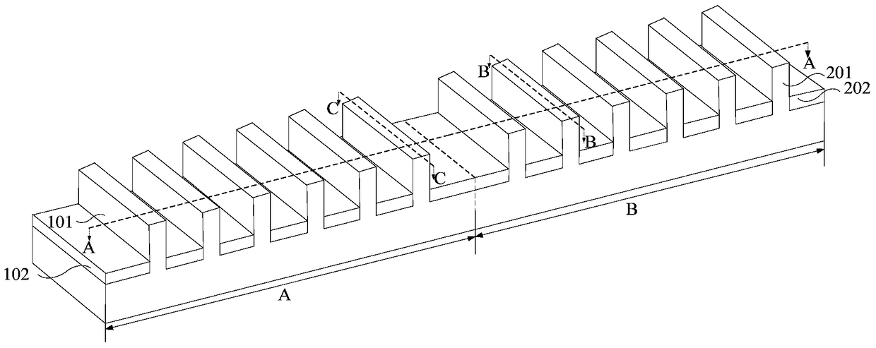
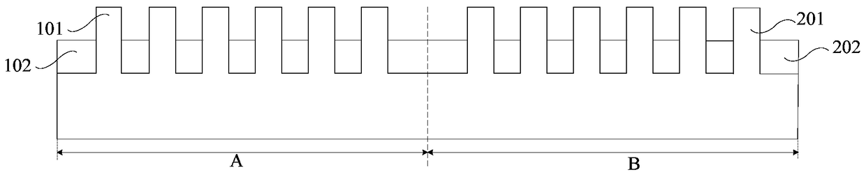
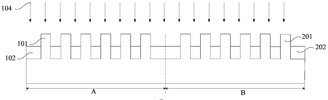
[0060] The device size (bulk width) of the FinFET is very small, especially, the top width (topwidth) of the fin and the bottom width (bottom width) of the fin. In prior art, refer to image 3 The ion implantation 104 of the semiconductor substrate in the peripheral region A, the fin portion 101 in the peripheral region and the semiconductor substrate in the core region B and the fin portion 201 in the core region is performed in one step. Ion implantation is first performed on the fin portion 201 of the core area to form a core area threshold voltage ion implantation layer. When the fin portion 201 of the core region is used to form an NMOS transistor, the implanted ions include phosphorus ions and arsenic ions. When the core region fin 201 is used to form a PMOS transistor, the implanted ions include boron ions. N...


PUM


Abstract

The invention discloses a forming method of a semiconductor device. The semiconductor device comprises a substrate, wherein the substrate comprises a peripheral region and a core region; the peripheral region is provided with a peripheral region fin part; the core region is provided with a core region fin part; a peripheral region ion implantation is carried out on the substrate of the peripheral region and the peripheral region fin part to form at least one of a peripheral region threshold voltage ion implantation layer and a peripheral region channel cutoff layer; first peripheral region gate structure material layers are formed in the substrate of the peripheral region and the peripheral region fin part; first core region gate structure material layers are formed on the substrate of the core region and the core region fin part; a core region ion implantation is carried out on the substrate of the core region and the core region fin part to form at least one of a core region threshold voltage ion implantation layer and a core region channel cutoff layer; and etching is respectively carried out on the first core region gate structure material layers and the second core region gate structure material layers to form a first core region gate structure and a second core region gate structure respectively. By the method disclosed by the invention, the performance of the semiconductor device can be improved.

Description

technical field [0001] The invention relates to the field of semiconductors, in particular to a method for forming a semiconductor device. Background technique [0002] With the continuous advancement of integrated circuits, that is, IC technology, the number of components integrated on the same chip has evolved from the initial tens of hundreds to the present millions. The performance and complexity of current ICs are far beyond what could have been imagined at the beginning. In order to meet the requirements of complexity and circuit density (that is, the number of devices integrated into a certain area), the minimum feature size, which is known as the "geometric line width" of the device, will become smaller and smaller with the innovation of process technology . [0003] As the feature size of transistors continues to shrink, the demand for smaller transistors is increasing, so fin field effect transistors are developed in transistor technology. [0004] refer to Fig...

Claims


Application Information

Patent Timeline
Patent Type & Authority Patents(China)
IPC IPC(8): H01L21/336
Inventor 李勇
Owner SEMICON MFG INT (SHANGHAI) CORP
Why Eureka
Try Eureka