Method of manufacturing semiconductor device

a manufacturing method and semiconductor technology, applied in the direction of coatings, transistors, chemical vapor deposition coatings, etc., can solve the problem of difficult to obtain a fine film containing less impurities, and achieve the effect of reducing the leakage current level of trench capacitors and excellent step coverag

Inactive Publication Date: 2007-03-22
SONY CORP
View PDF5 Cites 400 Cited by
  • Summary
  • Abstract
  • Description
  • Claims
  • Application Information

AI Technical Summary

Benefits of technology

[0015] In the embodiment of the method of manufacturing a semiconductor device according to the present invention, the capacitor insulating film of the trench capacitor is deposited in the form of the hafnium silicate film by utilizing the atomic layer deposition method using the hafnium raw material, the silicon raw material and the oxidizing agent. Hence, the concentration of the impurities such as carbon (C) contained in th

Problems solved by technology

A problem to be solved is that since the ALD method is utilized in the low temperatu

Method used


Image

  • Method of manufacturing semiconductor device
  • Method of manufacturing semiconductor device
  • Method of manufacturing semiconductor device

Examples


Embodiment Construction

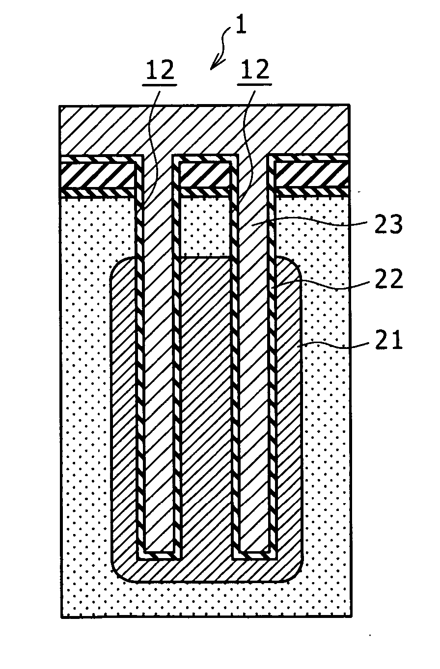
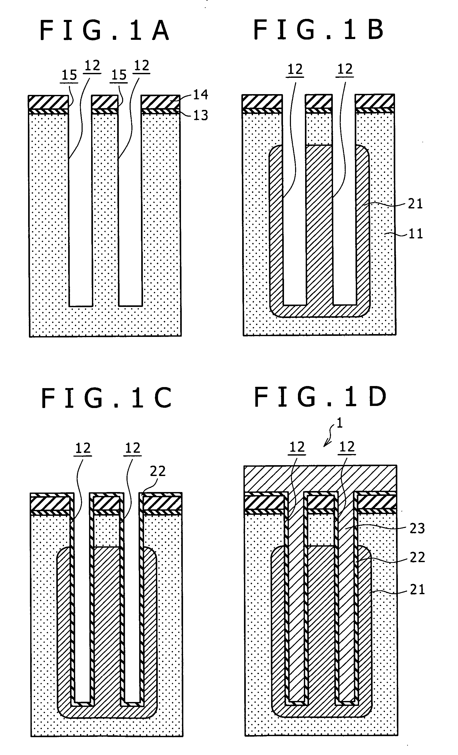
[0024] An embodiment according to a method of manufacturing a semiconductor device of the present invention will be described hereinafter in detail with reference to manufacturing process cross sectional views shown in FIGS. 1A to 1D, respectively. At that, since FIGS. 1A to 1D are schematically drawn, an aspect contraction scale ratio is not made to agree with an actual one.

[0025] As shown in FIG. 1A, trenches 12 in which a capacitor is intended to be formed are formed in a semiconductor substrate (or a semiconductor layer) 11. By the way, with regard to a method of forming the trench 12, there are the various kinds of existing methods. An example of the method of forming the trench 12 is as follows. That is to say, an oxide film 13 and a nitride film 14 are formed in this order on a surface of the semiconductor substrate (or the semiconductor layer) 11. After that, after a mask layer (not shown) which is used to form each trench is formed by utilizing a normal photolithography te...


PUM

PropertyMeasurementUnit
Temperatureaaaaaaaaaa
Pressureaaaaaaaaaa

Abstract

The invention aims at enabling leakage current characteristics and a step coverage property to be improved by depositing a hafnium silicate film by utilizing an atomic layer evaporation method using a hafnium raw material, a silicon raw material and an oxidizing agent. Disclosed herein is a method of manufacturing a semiconductor device having a trench capacitor including a first electrode formed on an inner surface of a trench, a capacitor insulating film formed on a surface of the first electrode, and a second electrode formed on a surface of the capacitor insulating film. The method includes the step of depositing the capacitor insulating film in a form of a hafnium silicate film by utilizing an atomic layer deposition method using a hafnium raw material, a silicon raw material and an oxidizing agent.

Description

CROSS REFERENCE TO RELATED APPLICATION [0001] The present invention contains subject matter related to Japanese Patent Application JP 2005-273145 filed in the Japanese Patent Office on Sep. 21, 2005, the entire contents of which being incorporated herein by reference. BACKGROUND OF THE INVENTION [0002] 1. Field of the Invention [0003] The present invention relates to a method of manufacturing a semiconductor device with which a capacitor insulating film of a trench capacitor having a deep trench can be readily formed of a hafnium silicate film having a low impurity concentration and having an excellent step coverage property. [0004] 2. Description of Related Art [0005] Along with scale down of semiconductor devices, the examination about application of a high dielectric constant film (a High-k film) to a material for each of a gate insulating film and a capacitor insulating film has been carried out. A lot of High-k films are made in the form of metallic oxides or silicate materials...

Claims


Application Information

Patent Timeline
IPC IPC(8): H01L21/8242
CPCC23C16/045C23C16/401H01L29/66181H01L21/3141H01L21/31645C23C16/45531H01L21/02148H01L21/0228
Inventor ANDO, TAKASHI
Owner SONY CORP
Why Eureka
Try Eureka