Process for producing metal thin films by ALD

a metal thin film and process technology, applied in the field of noble metal manufacturing methods, can solve the problems of difficult patterning platinum layers, poor adhesion of copper to diffusion barrier, easy oxidation, etc., and achieve the effect of improving uniformity of films and reproducibility of processes, promoting nucleation, and facilitating oxidation

Inactive Publication Date: 2005-01-27
ASM INTERNATIONAL
View PDF16 Cites 79 Cited by
  • Summary
  • Abstract
  • Description
  • Claims
  • Application Information

AI Technical Summary

Benefits of technology

[0025] The uniformity of the films and reproducibility of the processes can surprisingly be improved by providing the substrate surface with hydroxyl groups. Such a hydroxyl group rich surface, which promotes nucleation, can be realised very easily by depositing an ultra-thin layer of metal oxide, such as Al2O3 or TiO2. In one embodiment the layer of metal oxide is deposited by ALD by using H2O and / or H2O2 as an oxygen source.

Problems solved by technology

Although platinum has been widely used as an electrode material, many disadvantages are connected to that concept, For instance, it is very difficult to pattern platinum layers by etching and platinum catalyses the dissociation of O2 into atomic oxygen.
An evident challenge for these magnetic recording media applications is how to control the film thicknesses at an atomic layer level uniformly over large substrate areas.
Chemical methods, like chemical vapour deposition and atomic layer deposition, which could provide better step coverage for the copper seed layer, usually suffer from a poor copper to diffusion barrier adhesion.
Further, a general problem related to copper seeds is their easy oxidation, which necessitates a reduction step in the beginning of the electrodeposition process.
The main problem in the development work of depositing metals by ALD has been a lack of effective reducing agents, since the metal precursors applicable in ALD are typically compounds, where the metal is at a higher oxidation state (M. Ritala and M. Leskela, Atomic Layer Deposition, in Handbook of Thin Film Materials, Ed. H. S. Nalwa, Academic Press, San Diego (2001), Vol. 1, Chapter 2, p.
The growth temperature was varied from 230 to 315° C. and the growth rate was 25 nm / min at 315° C. However, carbon and hydrogen were incorporated as harmful impurities in the deposited films, thus increasing the resistivity of the film.
Furthermore, the general limitations of the CVD method, such as problems related to achieving good large area uniformity and accurate thickness control, still remain.
In addition, it is hard to obtain good step coverage and high film purity at the same time.

Method used


Image

  • Process for producing metal thin films by ALD
  • Process for producing metal thin films by ALD
  • Process for producing metal thin films by ALD

Examples


example 1

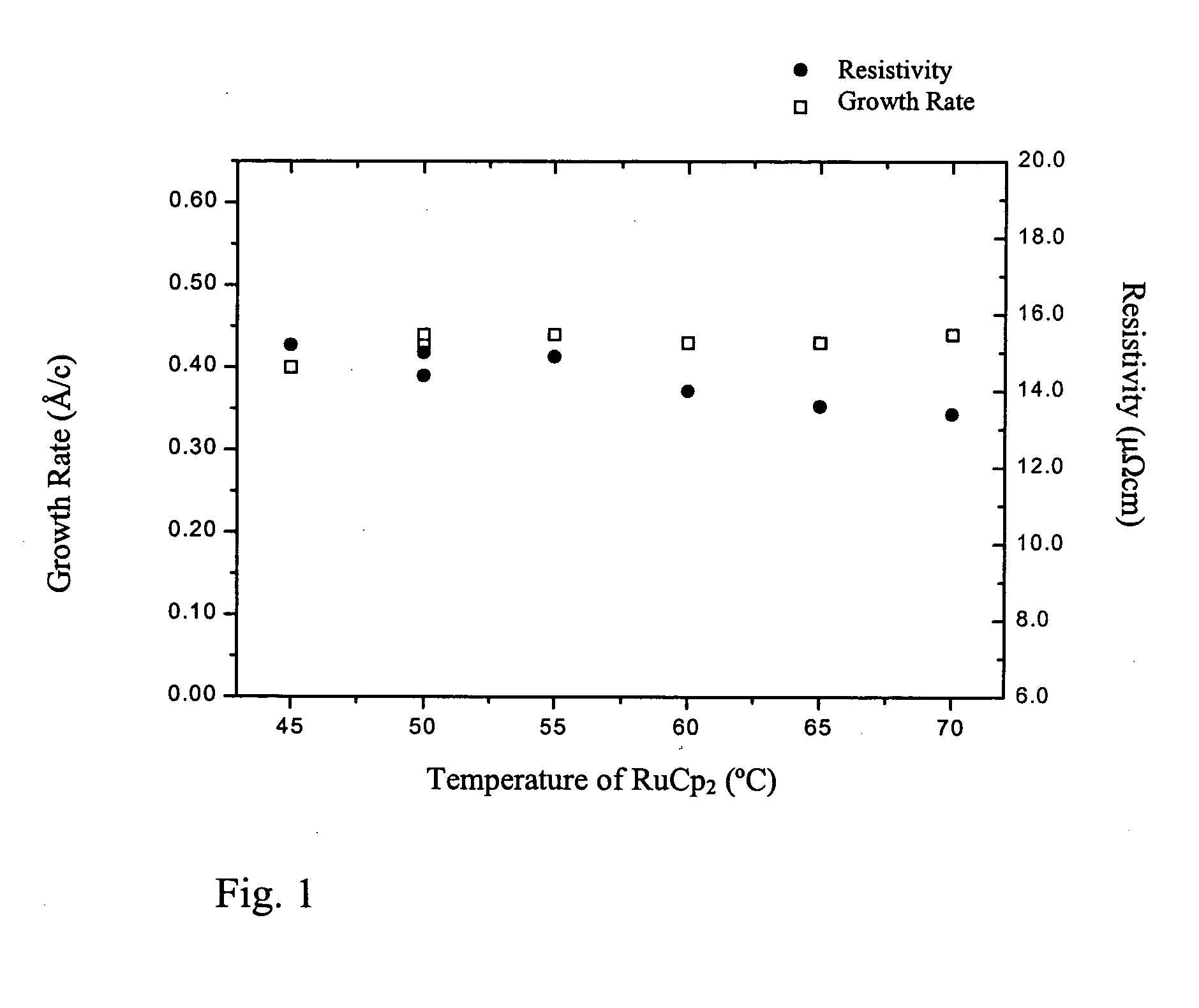
[0073] Ruthenium thin films were deposited in a flow type F-120 ALD reactor (ASM Microchemistry). Bis(cyclopentadienyl)ruthenium (Ru(Cp)2) and air (with a flow rate of 8 sccm during the pulses) were used as precursors. The ruthenium films were deposited on 5×5 cm2 borosilicate glass substrates covered by thin Al2O3 film. The growth temperature was 350° C.

[0074] The Al2O3 film was found to be beneficial to obtain uniform ruthenium films and a reproducible process. The inventors assume that this is due to a high density of reactive sites, such as hydroxyl groups (—OH), on an Al2O3 film. The density of such reactive sites is high on a fresh surface of an Al2O3 thin film that is deposited by ALD. In this experiment the thin Al2O3 film for initiating proper growth of Ru films was produced by ALD by using AlCl3 and H2O or H2O2 as precursors. Total amount of 40 cycles of Al2O3 was applied.

[0075] The effect of the dose of ruthenium precursor was varied by varying the evaporation temperatu...

example 2

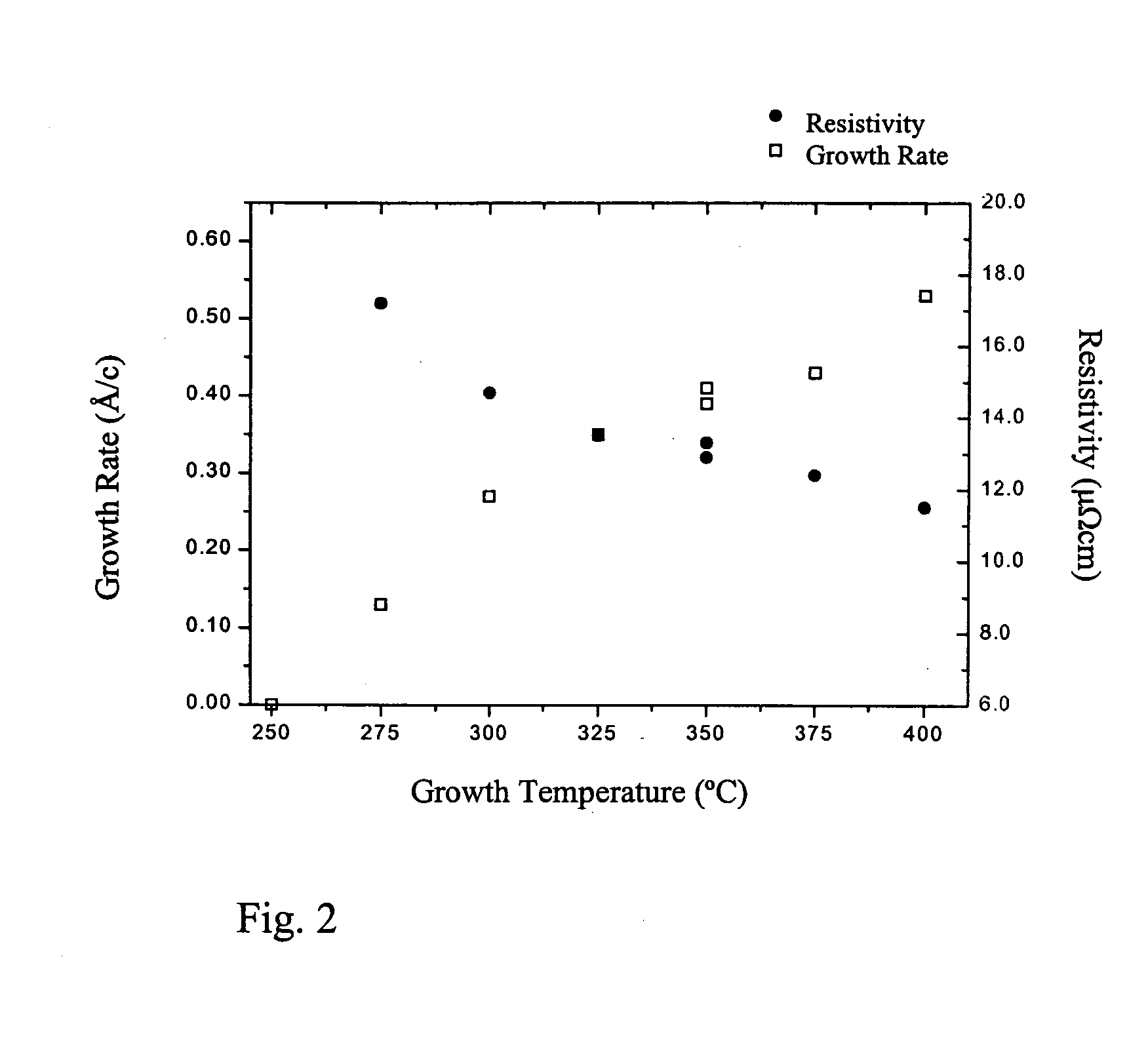
[0077] Ruthenium thin films were deposited in a flow type F-120 ALD reactor (ASM Microchemistry). Bis(cyclopentadienyl)ruthenium (Ru(Cp)2) and air (with a flow rate of 8 seem during the pulses) were used as precursors. Ru(Cp)2 was evaporated from an open boat inside the reactor at 50° C. The ruthenium films were deposited on 5×5 cm2 borosilicate glass substrates covered by thin Al2O3 film. The growth temperature was 350° C.

[0078] The effect of the dose of ruthenium precursor was varied by varying the pulse length of the evaporated precursor from 0.2 seconds to 1.2 seconds. The growth rate and the quality of the films were investigated.

[0079] The purge after the ruthenium pulse was 0.5 seconds. The pulse length of air pulse was 0.2 seconds and the purge thereafter was 0.5 seconds. The total amount of cycles was 3000.

[0080] The results in Table 1 show that the deposition rate is independent of the RuCp2 dose as varied through its pulse length, when the pulse time is longer than 0.2 ...

example 3

[0081] Ruthenium thin films were deposited in a flow type F-120 ALD reactor (ASM Microchemistry). Bis(cyclopentadienyl)ruthenium (Ru(Cp)z) and air were used as precursors. Ru(Cp)2 was evaporated from an open boat inside the reactor at 50° C. The ruthenium films were deposited on 5 cm×5 cm borosilicate glass substrates covered by thin Al2O3 film. The tested growth temperature was 350° C.

[0082] The pulse length of evaporated ruthenium precursor was 0.5 seconds and the purge thereafter was 0.5 seconds. The pulse length of air pulse was 0.2 seconds and the purge thereafter was 0.5 seconds. The total amount of cycles was 2000.

[0083] The effect of the dose of oxygen was tested by varying the air flow rate from 0 to 14 sccm. The growth rate and the quality of the films were investigated. The results in Table 2 show that the deposition rate is independent of the air flow above 4 sccm. This proves that the film growth proceeds in a self-limiting manner as characteristic to ALD. Further, as...


PUM

PropertyMeasurementUnit
thicknessaaaaaaaaaa
thicknessaaaaaaaaaa
thicknessaaaaaaaaaa

Abstract

The invention relates generally to processes for producing electrically conductive noble metal thin films on a substrate by atomic layer deposition. According to one embodiment of the invention a substrate with a surface is provided in a reaction chamber and a vaporised precursor of a noble metal is pulsed into the reaction chamber. By contacting the vaporised precursor with the surface of the substrate, no more than about a molecular layer of the metal precursor is formed on the substrate. In a next step, a pulse of molecular oxygen-containing gas is provided in the reaction chamber, where the oxygen reacts with the precursor on the substrate. Thus, high-quality metal thin films can be deposited by utilising reactions between the metal precursor and oxygen. In one embodiment, electrically conductive layers are deposited in structures that have high aspect ratio vias and trenches, local high elevation areas or other similar surface structures that make the surface rough.

Description

REFERENCE TO RELATED APPLICATIONS [0001] This application claims priority under 35 U.S.C. § 120 as a continuation of U.S. patent application Ser. No. 10 / 066,315, filed Jan. 29, 2002.BACKGROUND OF THE INVENTION [0002] 1. Field of the Invention [0003] This invention relates generally to methods of manufacturing noble metal (Ru, Rh, Pd, Ag, Re, Os, Ir, Pt) layers, such as for use in integrated circuits (IC) and magnetic recording media. [0004] 2. Description of the Related Art [0005] Ruthenium metal is considered to be one of the most promising materials for capacitor electrodes of dynamic random access memories (DRAMs) that have for example Ta2O5 and / or (Ba,Sr)TiO3 (BST) dielectrics. Ruthenium is also a potential electrode material for nonvolatile ferroelectric memories. Although platinum has been widely used as an electrode material, many disadvantages are connected to that concept, For instance, it is very difficult to pattern platinum layers by etching and platinum catalyses the di...

Claims


Application Information

Patent Timeline
Patent Type & Authority Applications(United States)
IPC IPC(8): C23C16/18C23C16/44C23C16/455G11B5/66G11B5/85H01F10/32H01L21/02H01L21/285H01L21/316H01L21/768H01L21/8242H01L21/8246H01L27/105H01L27/108
CPCB82Y25/00C23C16/18C23C16/45553G11B5/66H01L28/60H01F10/325H01L21/28562H01L21/3162H01L21/7687G11B5/85H01L21/0228H01L21/02183H01L21/02186C23C16/06
Inventor AALTONEN, TITTAALEN, PETRARITALA, MIKKOLESKELA, MARKKU
Owner ASM INTERNATIONAL
Why Eureka
Try Eureka