Recrystallization of semiconductor waters in a thin film capsule and related processes

Active Publication Date: 2010-11-25
MASSACHUSETTS INST OF TECH
View PDF13 Cites 18 Cited by
  • Summary
  • Abstract
  • Description
  • Claims
  • Application Information

AI Technical Summary

Benefits of technology

[0009]The crystal structure of the wafer is then improved 122 by passing it through a furnace, which creates a region in space where a molten zone arises, through which the wafer travels, resulting in recrystallization, a new and improved crystal structure. The furnace may consist of heater rods and insulation brick. The cooling zone of the furnace must be well controlled to minimize thermally induced stresses and the crystallographic defects caused by them.
[0010]The thin film capsule contains the molten material during the recrystallization. It also aids in retaining the shape of the original wafer, although support or backing plates may be required to establish flatness of the product. The thin film capsule acts as a diffusion barrier ag

Problems solved by technology

This preform original wafer can, and typically would, consist of ver

Method used


Image

  • Recrystallization of semiconductor waters in a thin film capsule and related processes
  • Recrystallization of semiconductor waters in a thin film capsule and related processes
  • Recrystallization of semiconductor waters in a thin film capsule and related processes

Examples


Embodiment Construction

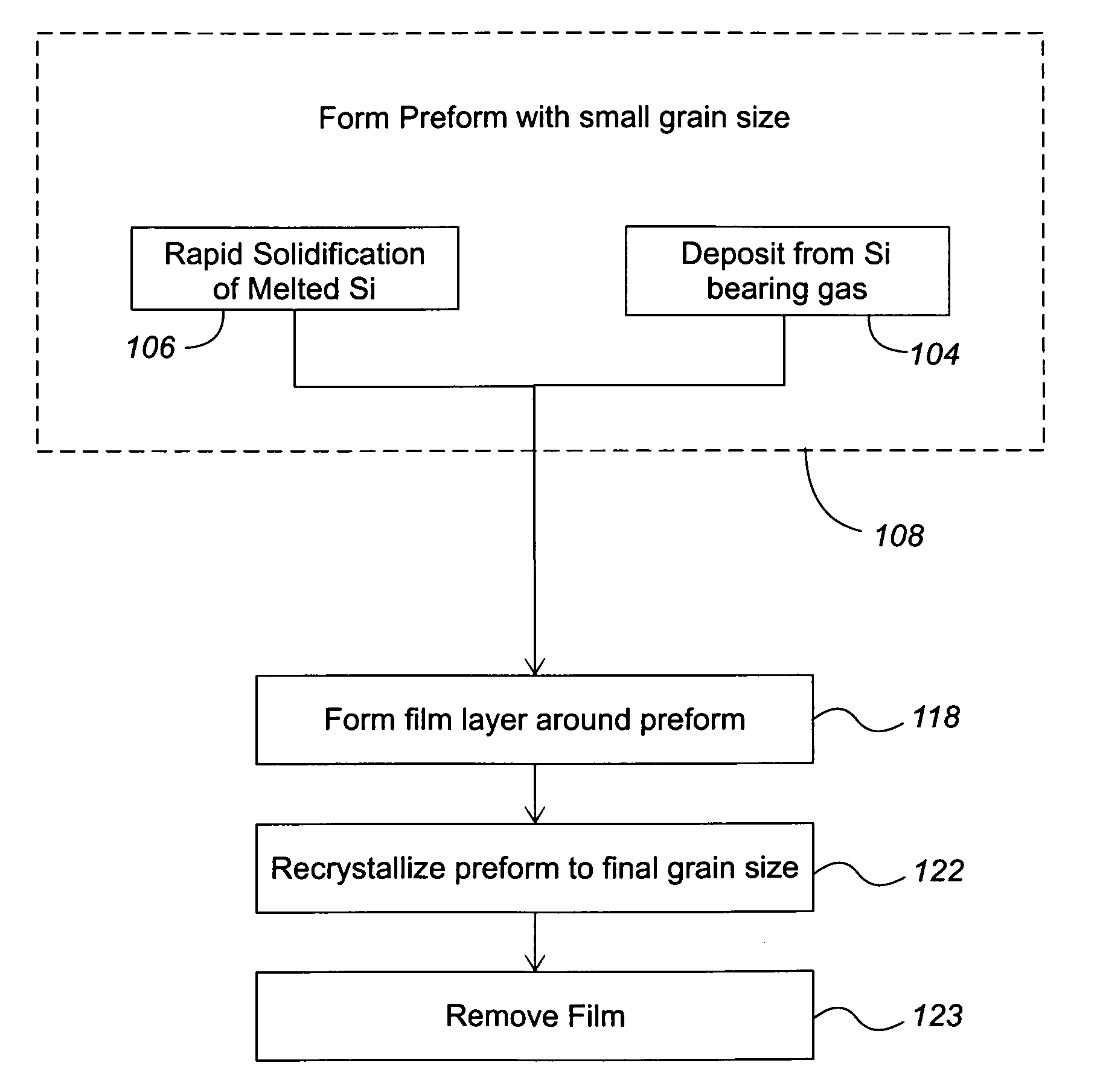
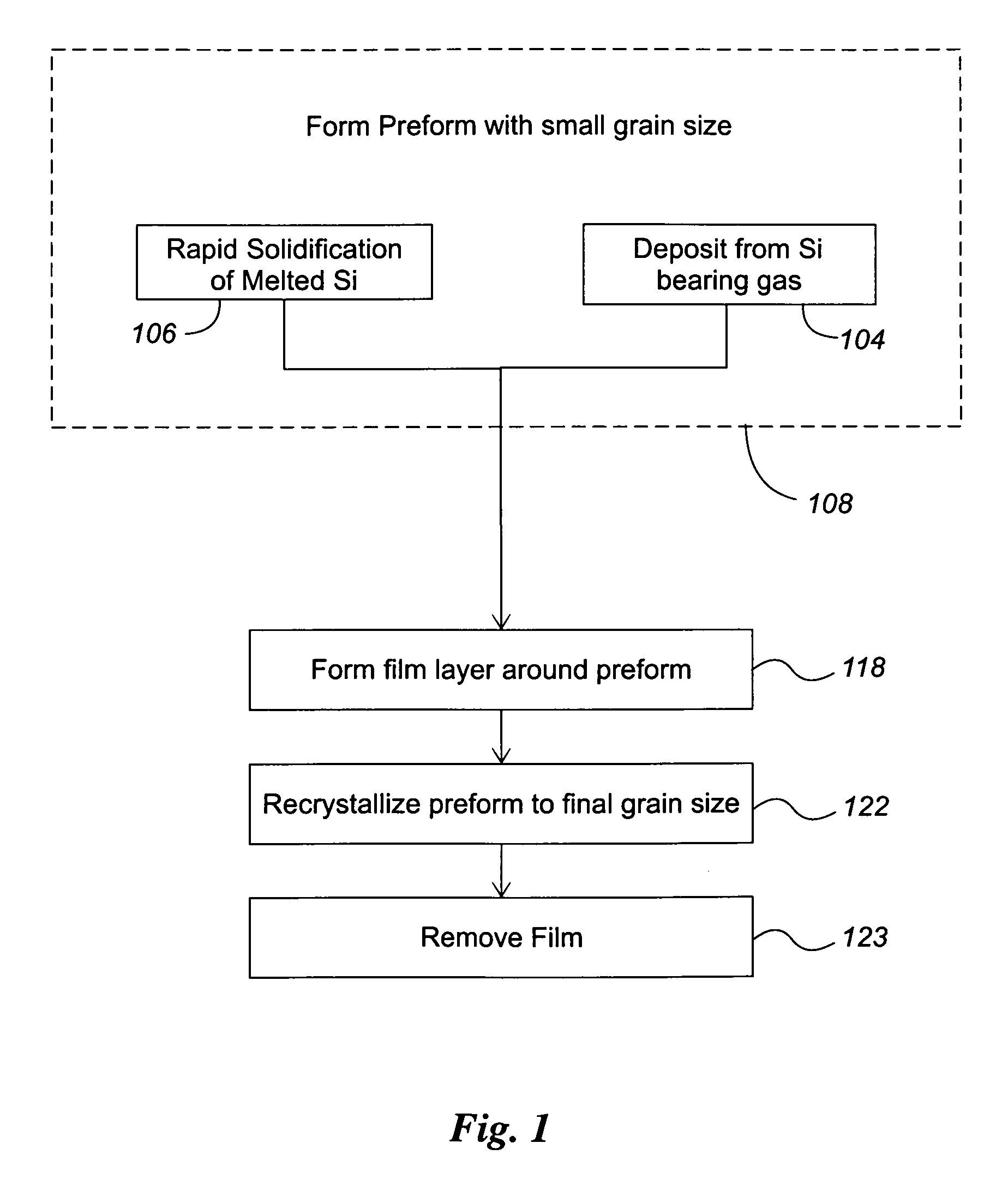
[0043]One approach disclosed herein, is to manufacture silicon wafers with no sawing required, by first creating the geometric form of the wafer and then, in a separate process, creating the desired crystallographic structure. (The sequence is the reverse of ingot methods where the crystallographic structure is created and then, through sawing, the geometric form is created).

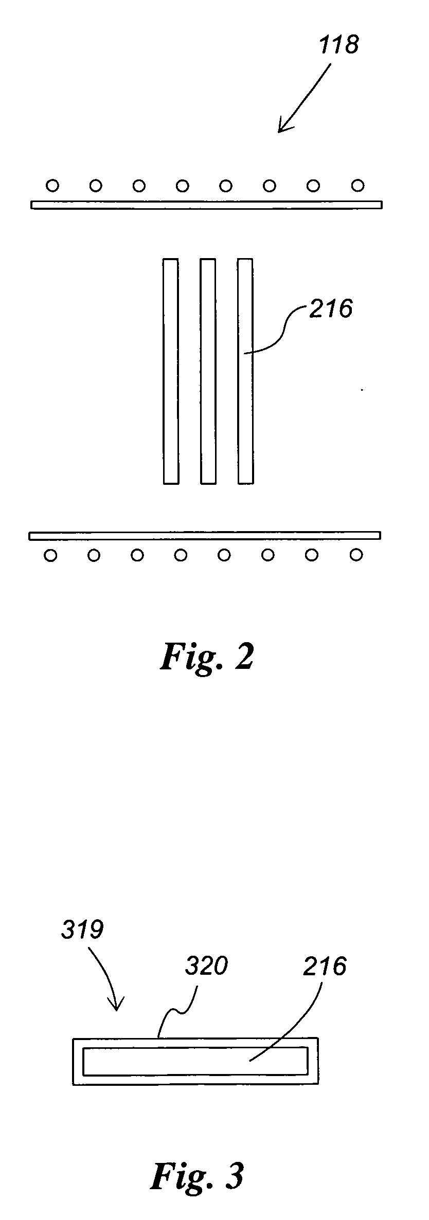
[0044]An overview of a process is shown with reference to FIG. 1 in flowchart form, and with reference to FIGS. 2 and 3 at various stages of production. As shown in FIG. 1, the geometric form of the wafer may be created in step 108. For instance, rapid solidification techniques 106 can be used, as discussed below. Alternatively, chemical vapor deposition techniques 104 can be used. This results in an original wafer having an average grain size of less than about ten mm2, and typically, less that about one mm2.

[0045]As shown schematically in FIGS. 2 and 3, in an important step, a super-clean, thin film capsule 32...


PUM


Abstract

An original wafer, typically silicon, has the form of a desired end PV wafer. The original may be made by rapid solidification or CVD. It has small grains. It is encapsulated in a clean thin film, which contains and protects the silicon when recrystallized to create a larger grain structure. The capsule can be made by heating a wafer in the presence of oxygen, or steam, resulting in silicon dioxide on the outer surface, typically 1-2 microns. Further heating creates a molten zone in space, through which the wafer travels, resulting in recrystallization with a larger grain size. The capsule contains the molten material during recrystallization, and protects against impurities. Recrystallization may be in air. Thermal transfer through backing plates minimizes stresses and defects. After recrystallization, the capsule is removed.

Description

RELATED DOCUMENTS[0001]The benefit of U.S. Provisional application No. 60 / 937,129, filed on Jun. 26, 2007, entitled Casting and Directional Solidification of Photovoltaic Silicon Wafers in a Capsule and Related Processes, is hereby claimed, and the entire disclosure is hereby incorporated fully herein, by reference.INTRODUCTION[0002]Crystalline silicon wafers (both single-crystal and multi-crystalline) are the basic building block in the vast majority of photovoltaic modules being manufactured today. Except for the small market share held by ribbon silicon, all these wafers are made by sawing up ingots. Sawing is itself quite expensive and, in addition, wastes over half of the expensive silicon raw material to sawn dust. The result is that the cost of the wafer accounts for almost half the cost of manufacturing a photovoltaic module.[0003]Ribbon approaches, on the other hand, produce material which is less flat and more highly defected than ingot-sawn wafers. The high temperature gr...

Claims


Application Information

Patent Timeline
IPC IPC(8): H01L29/12H01L21/02H01L29/24
CPCC30B1/02C30B28/02C30B29/06H01L21/02532H01L21/02667H01L29/04H01L2924/0002H01L23/3171C30B13/00H01L2924/00H01L21/324
Inventor SACHS, EMANUEL M.SERDY, JAMES G.HANTSOO, EERIK T.
Owner MASSACHUSETTS INST OF TECH
Why Eureka
Try Eureka