Method for fabricating semiconductor device and forming interlayer dielectric film using high-density plasma

a technology of interlayer dielectric film and high-density plasma, which is applied in the direction of semiconductor devices, semiconductor/solid-state device details, electrical equipment, etc., can solve the problems of physical cracking around the void, inability to use during the process of fabricating a highly integrated semiconductor device in which a high temperature process is not available, and easy formation of porous defects between gates

Inactive Publication Date: 2005-03-15
SAMSUNG ELECTRONICS CO LTD
View PDF11 Cites 82 Cited by
  • Summary
  • Abstract
  • Description
  • Claims
  • Application Information

AI Technical Summary

Benefits of technology

To solve the above problem, an objective of the present invention is to provide methods for fabricating a semiconductor device and forming an interlayer die

Problems solved by technology

Borophospho-silicate glass, which has a high flowability at high temperature; has usually been used as an interlayer dielectric film formed between gates, but it cannot be used during a process of fabricating a highly integrated semiconductor device in which a high temperature process is not available.
However, when using the interlayer dielectric film formed

Method used


Image

  • Method for fabricating semiconductor device and forming interlayer dielectric film using high-density plasma
  • Method for fabricating semiconductor device and forming interlayer dielectric film using high-density plasma
  • Method for fabricating semiconductor device and forming interlayer dielectric film using high-density plasma

Examples


Embodiment Construction

The above objective and advantages of the present invention will become apparent by describing in detail preferred embodiments thereof with reference to the appended drawings. While the present invention has been particularly shown and described with reference to the preferred embodiment(s) thereof, the present invention is not restricted to the embodiments. The embodiments of the present invention are provided to help those skilled in the art to completely understand the present invention.

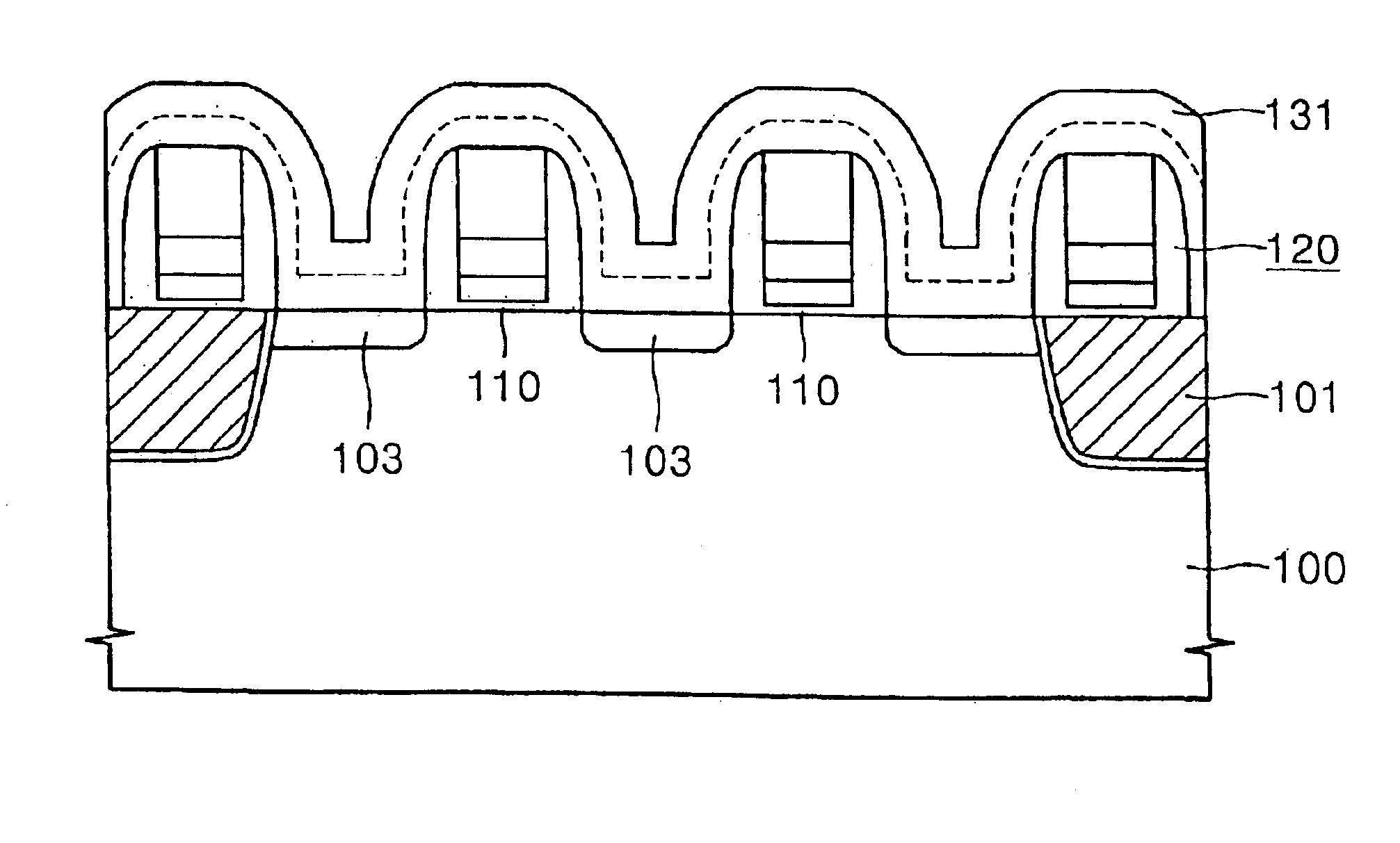
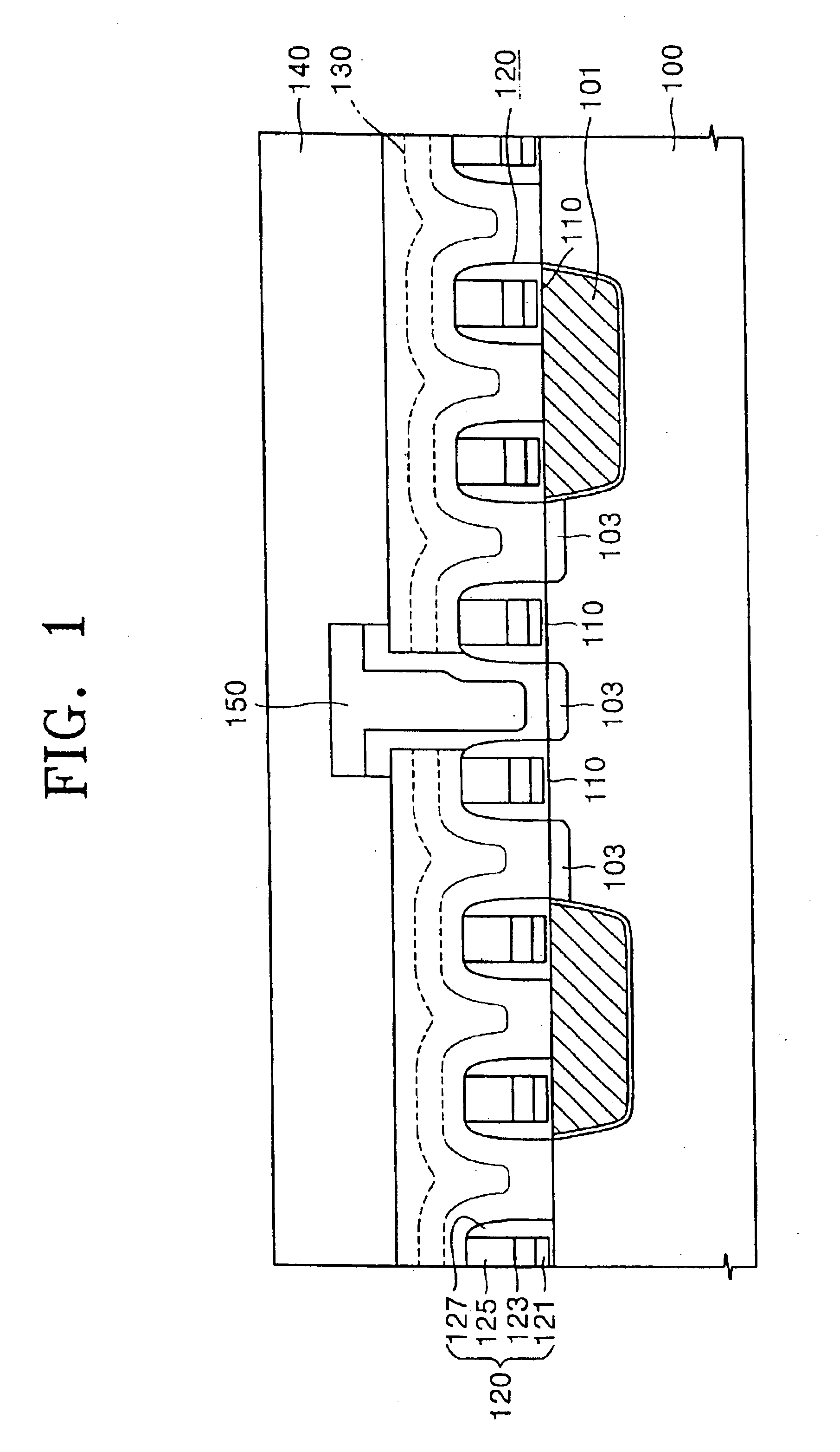
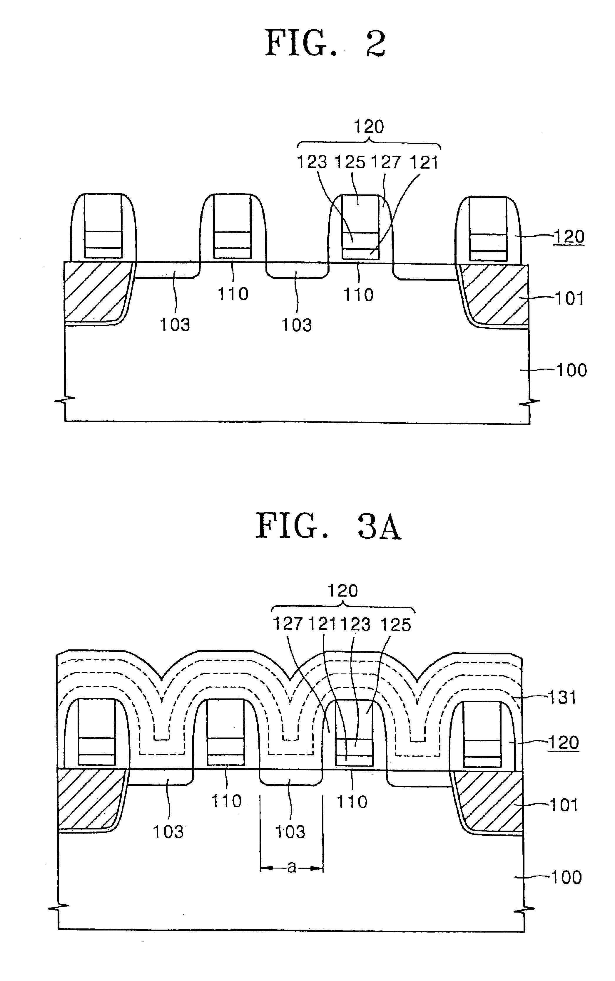
FIG. 1 shows a cross-section of a semiconductor device made through a method of fabricating a semiconductor device according to an embodiment of the present invention. In the semiconductor device shown in FIG. 1, trenches each having a predetermined depth are formed in a semiconductor wafer 100 made of a silicon substrate. Each of the trenches is filled with an insulating film, thereby forming an isolation oxide film 101 for isolating devices from each other. Source / drain junctions 103 are formed ...


PUM


Abstract

A method for fabricating a semiconductor device and forming an insulating film used therein, includes forming an isolation insulating film on a semiconductor wafer and forming gates, separated by gaps having a predetermined distance, on an active region. Next, a first interlayer dielectric film is deposited to a predetermined thickness on the semiconductor wafer having the gates, so that the gaps between the gates are not completely filled. Then, a sputtering etch is performed entirely on a surface of the first interlayer dielectric film. Thereafter, the first interlayer dielectric film is partially removed through isotropic etching. Next, a second interlayer dielectric film is deposited on the first interlayer dielectric film so that the gaps between the gates are completely filled. According to the above method, a gap between gate patterns can be completely filled without a void by performing sputtering etch on interlayer dielectric films formed on gate patterns, thereby enhancing the reliability of a semiconductor device.

Description

BACKGROUND OF THE INVENTION1. Field of the InventionThe present invention relates to a method for fabricating a semiconductor device and forming an interlayer dielectric film, and more particularly, to a method for forming an interlayer dielectric film using high-density plasma.2. Description of the Related ArtAs the integration density of semiconductor devices increases, the distance between devices gets narrower. Thus the critical dimensions of the gate of a MOS transistor, which is one of the main constituents for a semiconductor device, become very small. As a result, the distance between gates becomes shorter. Moreover, since self-aligned contacts are made in highly integrated semiconductor devices such as DRAM cells, the height of a gate can be sufficiently increased, but the depth of a gap between gates is comparatively deep compared to the width of the gate. In this regard, it has been a matter of concern to fill a gap between gates with an insulating film.Borophospho-silica...

Claims


Application Information

Patent Timeline
IPC IPC(8): H01L21/70H01L21/02H01L21/768H01L21/316H01L21/3105H01L21/8234H01L21/31H01L21/8242H01L23/522H01L27/108
CPCH01L21/02164H01L21/02211H01L21/02274H01L21/31055H01L21/31612H01L21/76819H01L21/76832H01L21/76837H01L21/823425H01L21/76801Y10S438/958H01L21/31
Inventor JUNG, WOO CHANLEE, JONG KOO
Owner SAMSUNG ELECTRONICS CO LTD
Why Eureka
Try Eureka