Chip and multi-chip semiconductor device using thereof and method for manufacturing same

a semiconductor device and chip technology, applied in semiconductor devices, semiconductor/solid-state device details, electrical apparatus, etc., can solve the problems of inability to provide sufficient level of dimensional accuracy in alignment, inability to align fine-pitch bonding alignment, poor alignment accuracy, etc., to achieve the effect of reducing the noise emitted by the chip during the operation of the multi-chip semiconductor device, reducing the diameter of the via, and improving the reliability

Inactive Publication Date: 2006-10-17
RENESAS ELECTRONICS CORP
View PDF8 Cites 370 Cited by
  • Summary
  • Abstract
  • Description
  • Claims
  • Application Information

AI Technical Summary

Benefits of technology

[0032]According to the bonding apparatus for the chip for the multi-chip semiconductor device of the present invention, the alignment accuracy can be improved when the chip for the multi-chip semiconductor device and the other chip are stacked by employing the bonding apparatus. For example, the bonding can be conducted at an alignment accuracy level of finer than 1 μm.
[0049]Moreover, the diameter of the vias can be considerably reduced by utilizing the dry etching in the aforementioned process of etching the vias in the method for manufacturing the chip according to the present invention, as compared with the case of forming a through hole by other procedures such as laser processing or drilling that present the through hole having a diameter of at least several tens μm. Thus, the chip having further improved aligning accuracy can be stably manufactured via the simple and easy process.

Problems solved by technology

On the other hand, when the diameter of the through hole is larger, an accuracy of the alignment is worse even though sufficient intensity of light is acquired.
Therefore, the method cannot provide sufficient level of the dimensional accuracy in the alignment, and thus the alignment for the fine pitch bonding is impossible in such method.
Similarly, the method of drawing the marking onto the backside of the chips corresponding to the positions of the electrodes on the surfaces of the chips, described in Japanese Patent Laid-Open No. 2000-228488, cannot achieve an accurate positioning control at the accuracy level of not finer than 1 μm.
Therefore, the lower chip is hidden behind the upper chip when chips having an identical size are stacked, such that the marking for alignment cannot be recognized, and thus the application of this method is difficult in such condition.

Method used


Image

  • Chip and multi-chip semiconductor device using thereof and method for manufacturing same
  • Chip and multi-chip semiconductor device using thereof and method for manufacturing same
  • Chip and multi-chip semiconductor device using thereof and method for manufacturing same

Examples


first embodiment

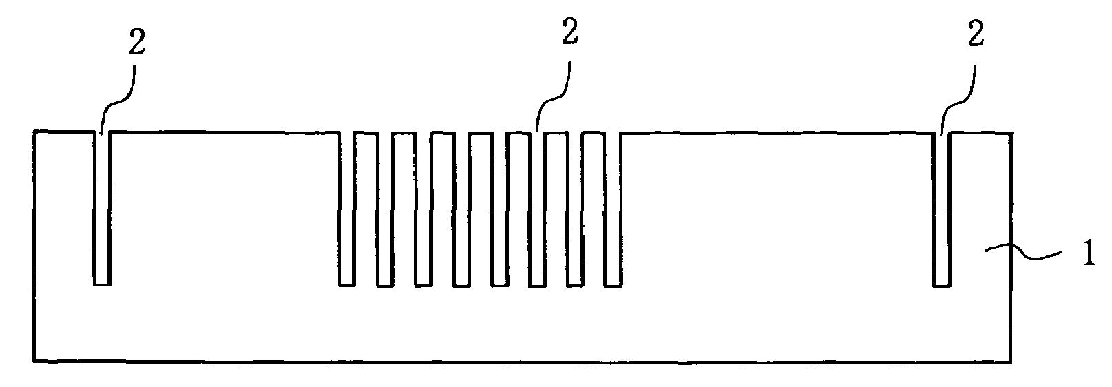
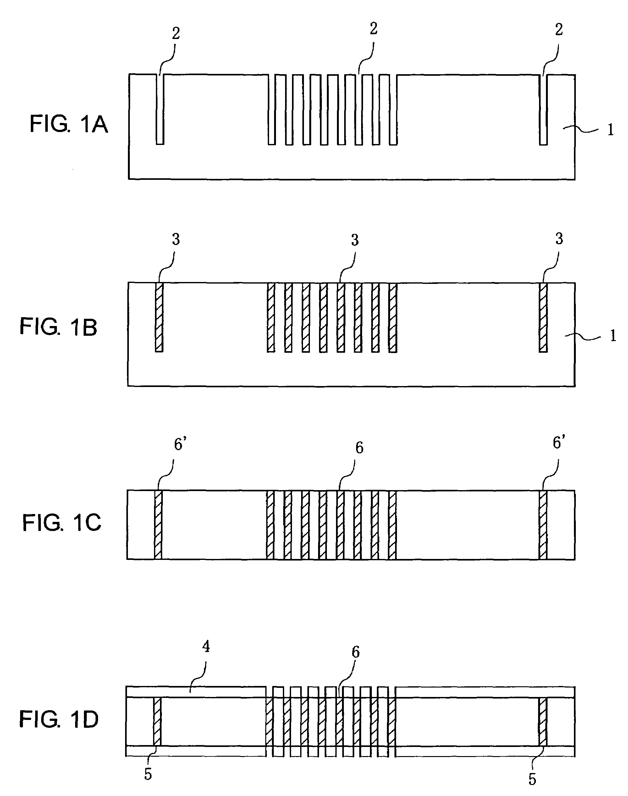
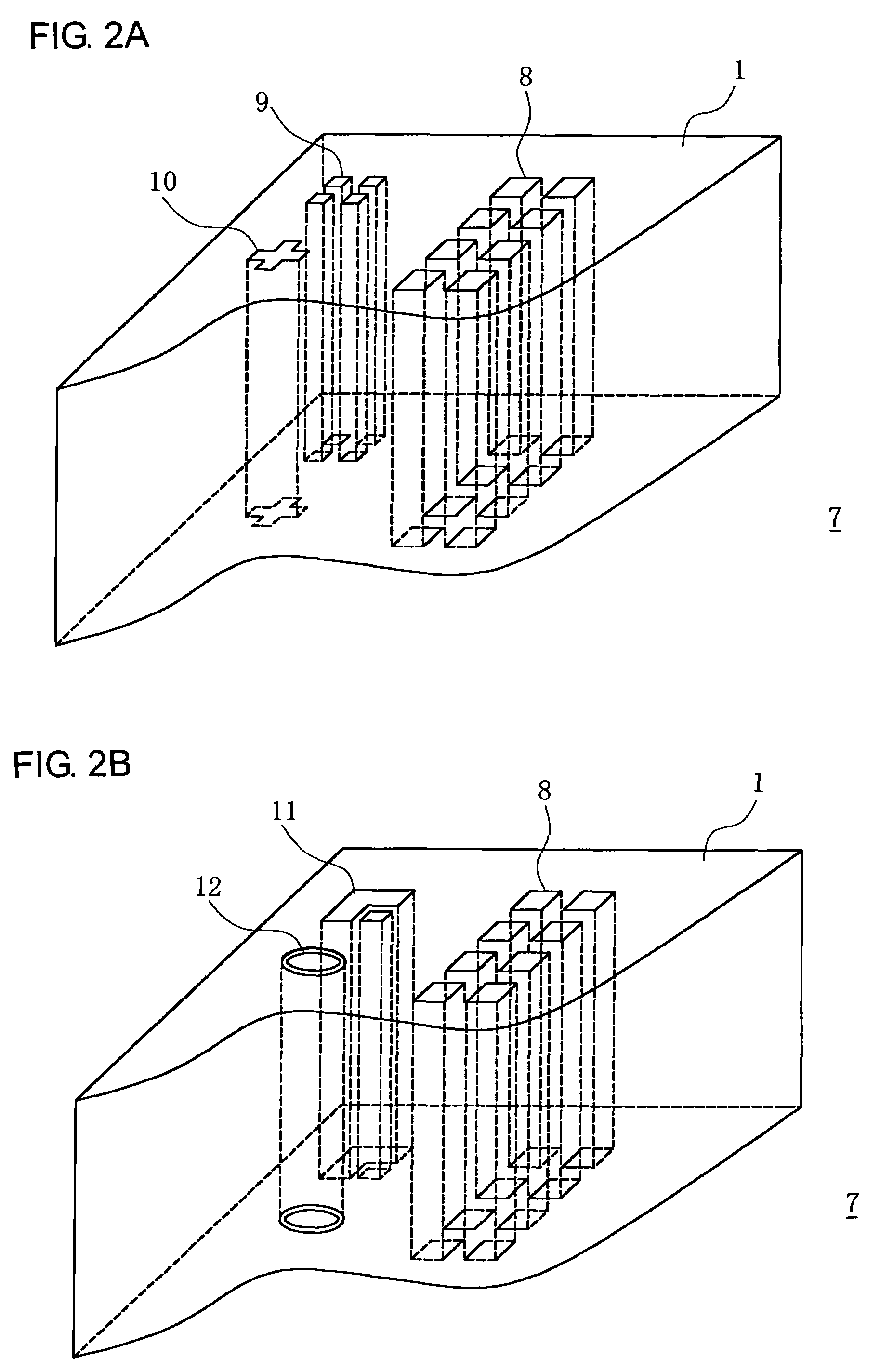
[0066]FIG. 2A and FIG. 2B are perspective views, illustrating a configuration of a chip for a multi-chip semiconductor device of the present embodiment. A chip 7 for a multi-chip semiconductor device shown in FIG. 2A and FIG. 2B is a chip composing the multi-chip semiconductor device, which includes a plurality of stacked semiconductor chips, and comprises a substrate 1 (silicon substrate), and a plurality of electroconductive through plugs that are composed of a conductive material passing through the substrate 1 (electroconductive through plugs 8 and markings for alignment 9 to 12).

[0067]These multiple electroconductive through plugs comprise first electroconductive through plugs (electroconductive through plugs 8) and second electroconductive through plugs that are provided separately from the electroconductive through plugs 8 (markings for alignment 9 to 12). The markings for alignment 9 to 12 and the electroconductive through plugs 8 are configured to be visually distinctive in...

second embodiment

[0093]FIG. 3 is a plan view, illustrating a configuration of a chip for a multi-chip semiconductor device of the present embodiment. A chip for a multi-chip semiconductor device (chip 13) shown in FIG. 3 comprises electroconductive through plugs 14 to 16, markings for alignment 17 and markings for alignment 18. The chip 13 can be manufactured by using, for example, a method for manufacturing the chip for the multi-chip semiconductor device described in the first embodiment.

[0094]In FIG. 3, a two-dimensional geometry of the chip 13 is a rectangular (square in this embodiment).

[0095]The marking for alignment 17 appeared in the lower portion in FIG. 3 and the marking for alignment 18 appeared in the upper portion thereof are illustrated to be asymmetrically arranged within the surface of the chip 13 (in the upper and the lower portions in the figure). More specifically, a configuration is provided, in which the lower markings for alignment 17 and the upper marking for alignment 18 are ...

third embodiment

[0099]In the third embodiment, a configuration of providing an identification of the marking for alignment is presented by utilizing the relative position of an electroconductive through plug functioning as a marking for alignment against an electroconductive through plug functioning as a though electrode within the surface of a substrate.

[0100]FIGS. 4A to 4G are plan views, illustrating a configuration of a chip for a multi-chip semiconductor device of the present embodiment. In FIGS. 4A to 4G, electroconductive through plugs and alignment markings are shown, and the substrate is not shown. A chip for a multi-chip semiconductor device shown in FIGS. 4A to 4G can be manufactured by, for example, using any of the aforementioned methods for manufacturing the chip for the multi-chip semiconductor device.

[0101]FIG. 4A to FIG. 4D illustrate examples of providing identifications by forming alignment markings having a two-dimensional geometry same as that of electroconductive through plugs...


PUM


Abstract

The chip for the multi-chip semiconductor device having the markings for alignment formed on the front surface and / or the back surface of the chip only by the processing from the front surface of the chip (photolithography, etch) and the method for manufacturing same are presented, without adding any dedicated process step to the formation process for the marking for alignment. In the chip for the multi-chip semiconductor device having two or more electroconductive through plug in one chip for the multi-chip semiconductor device, one or more electroconductive through plugs are employed for the marking for alignment, and the chip is configured to allow identification of the marking for alignment on the front surface and / or the back surface of the chip for the multi-chip semiconductor device. Then, an insulating film is provided on the front surface and / or the back surface of the electrically conducting through plug.

Description

[0001]The present application is based on Japanese Patent Application NO.2004-020444, filed Jan. 28, 2004 the whole disclosure of which is hereby incorporated by reference.BACKGROUND OF THE INVENTION[0002]1. Field of the Invention[0003]The present invention relates to a chip for a multi-chip semiconductor device having a marking for alignment and a multi-chip semiconductor device employing thereof, and to a method for manufacturing same.[0004]2. Background of the Art[0005]In recent years, semiconductor chips (hereinafter referred to as simply “chips”) having very large scale integrated circuit (VLSI) are frequently employed for forming critical portions in computers and communication equipments. The conformation of forming a stacked body of a plurality of chips is often employed among the usage of such chips. Here, when a plurality of chip is employed to form a stacked body, the particularly critical point may be how the positions of the respective chips are adjusted, or namely the ...

Claims


Application Information

Patent Timeline
Patent Type & Authority Patents(United States)
IPC IPC(8): H01L23/544H01L23/02H01L25/18H01L21/60H01L21/98H01L23/48H01L23/498H01L23/52H01L25/065H01L25/07
CPCH01L23/481H01L23/49827H01L23/49833H01L23/544H01L24/81H01L25/0657H01L25/50H01L2223/54473H01L2224/81801H01L2225/06513H01L2225/06541H01L2225/06593H01L2924/01013H01L2924/01029H01L2924/01033H01L2924/01078H01L2924/01079H01L2924/01082H01L2924/14H01L2924/15311H01L2924/19041H01L2924/19042H01L2924/19043H01L2924/30105H01L2924/01005H01L2924/01006H01L2924/0105H01L2924/01074H01L2924/014H01L2224/16145Y10S438/975H01L2224/81136H01L2224/05573H01L2224/05611H01L2224/05624H01L2224/05644H01L2224/05647H01L2224/05666H01L2224/05684H01L2224/13025H01L2224/16146H01L2224/16225H01L2224/17181H01L2924/12042H01L2924/00H01L2924/00014
Inventor MATSUI, SATOSHI
Owner RENESAS ELECTRONICS CORP
Why Eureka
Try Eureka