Alignment method for attaching chip or flexible circuit board to circuit substrate

A technology of flexible circuit boards and circuit substrates, which is applied in the direction of circuits, electrical components assembly printed circuits, electrical components, etc., which can solve the problems of the influence of the accuracy of the display substrate's shape and size, and the inability to meet the requirements of high-precision alignment.

Active Publication Date: 2011-08-24
苏州凯蒂亚半导体制造设备有限公司
View PDF5 Cites 40 Cited by
  • Summary
  • Abstract
  • Description
  • Claims
  • Application Information

AI Technical Summary

Problems solved by technology

Obviously, this method cannot meet the high-precision alignment requirements due to the influence of the dimension accuracy of the display substrate.

Method used


Image

  • Alignment method for attaching chip or flexible circuit board to circuit substrate
  • Alignment method for attaching chip or flexible circuit board to circuit substrate
  • Alignment method for attaching chip or flexible circuit board to circuit substrate

Examples


Embodiment

[0182] Embodiment: a kind of aligning method of sticking drive chip on the display screen substrate of a flat panel display, its content is as follows:

[0183] (1) Alignment reference and alignment method

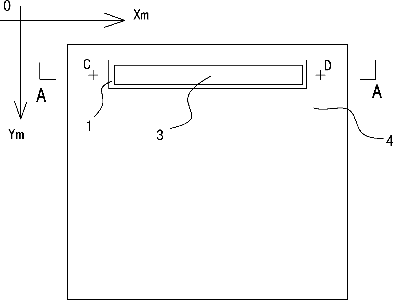
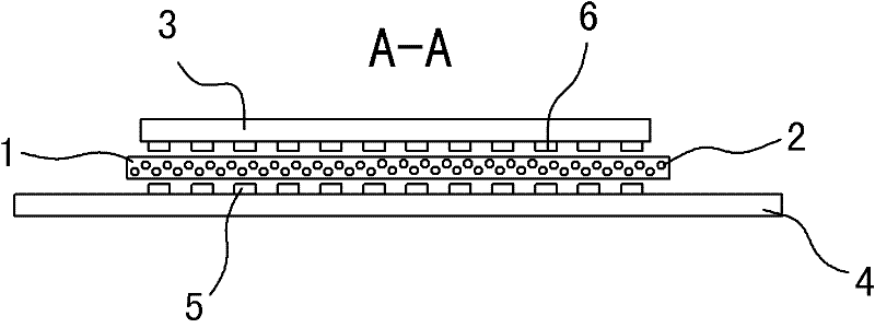
[0184] In driver chip 3 (see figure 1 and figure 2 ) The horizontal mechanical coordinate system M where the mounting plane is located (see figure 1 and figure 2 In the mechanical coordinate system drawn in ), with the position and direction of the driver chip 3 as the reference, the drive pin 6 on the driver chip 3 and the display are realized by adjusting the position and direction of the display substrate 4 (such as an LCD liquid crystal panel) Alignment of the driving terminals 5 on the screen substrate 4 .

[0185] (2) Adjustment method

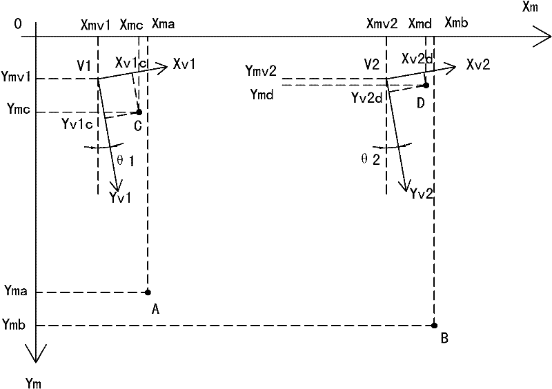
[0186] Make two marking points for alignment on the display substrate 4 in advance, namely the first marking point C and the second marking point D (see figure 1 ), these two identification points can be used for image rec...


PUM


Abstract

The invention discloses an alignment method for attaching a chip or a flexible circuit board to a circuit substrate, which is characterized by comprising the following steps of: designing two identification points on the circuit substrate in advance; after the circuit substrate is transferred to a framing table board and positioned, shooting images of the two identification points by using a camera, converting the images of the two identification points into position coordinates of an image coordinate system by using an image processing system; converting image coordinates of the two identification points into mechanical coordinate values of a mechanical coordinate system by using a relationship between the image coordinate system and the mechanical coordinate system; finding out an X-directional offset, a Y-directional offset and a deflection angle around a Z axis between the actual positions of the two identification points and a target position through calculation; and finally adjusting the two identification points to the target position by using an X-directional movement mechanism, a Y-directional movement mechanism and a rotating mechanism around the Z axis, so that the chip or the flexible circuit board is aligned with a conducting terminal of the circuit substrate. By the invention, the alignment precision of a chip on glass (COG), a film on glass (FOG) and a chip on film (COF) is greatly improved.

Description

technical field [0001] The invention relates to the technical field of flat-panel display manufacture, in particular to an alignment method in COG, FOG and COF thermal compression bonding. The COG (that is, CHIP ON GLASS) refers to the loading process that uses ACF film to directly bind the chip on the liquid crystal display through hot pressing. The FOG (ie, FILM ON GLASS) refers to the mounting process of directly binding the flexible circuit board on the liquid crystal display by using ACF film through hot pressing. The COF (that is, CHIP ON FILM) refers to the mounting process that uses ACF film to directly bind the chip on the flexible circuit board through hot pressing. The so-called ACF film (Anisotropic Conductive Film) is an anisotropic conductive film, which is a film with conductive particles scattered on an adhesive resin. Background technique [0002] Applied to COG, FOG and COF thermal compression bonding technology, such as correctly assembling the driver ch...

Claims


Application Information

Patent Timeline
Patent Type & Authority Applications(China)
IPC IPC(8): H05K3/30H05K3/32H01L21/50H01L21/60H01L21/66
CPCH01L2224/83101
Inventor 陈华轩景建平唐志稳朱晓伟
Owner 苏州凯蒂亚半导体制造设备有限公司
Why Eureka
Try Eureka