Wiring board, mount structure, and method for manufacturing the same

a technology of mounting structure and wiring board, which is applied in the direction of inspection/indentification of circuits, instruments, optics, etc., can solve the problems of mounting failure, significant expansion or contraction of wiring board, and change the pitch of connecting terminal array, so as to simplify alignment work and high general versatility

Active Publication Date: 2007-11-29
JAPAN DISPLAY WEST
View PDF11 Cites 40 Cited by
  • Summary
  • Abstract
  • Description
  • Claims
  • Application Information

AI Technical Summary

Benefits of technology

[0027]With this structure, even if the pitch of the mounting-object-side terminals and the pitch of the wiring-board-side terminals are displaced by the expansion or contraction of the wiring board or the mounting object, the wiring-board-side terminals and the mounting-object-side terminals can be properly agreed irrespective of the expansion or contraction of the wiring board when the first portions of the wiring board and the first portions of the mounting object are partially agreed in the extending direction. This method eliminates the need for the operator to independently determine the amount of expansion or contraction of the wiring board, thus offering high general versatility and contributing to simplification of alignment work.

Problems solved by technology

However, the wiring board expands or contracts significantly because it is basically made of polyimide resin, which changes the pitch of the connecting terminal array.
This causes disagreement of the positions of the connecting terminal array and the input terminal array, thus posing the problem of mount failure.
However, the alignment method using the reference mark and the scale requires the operator to determine the amount of the expansion or contraction of the wiring board, thus posing the problem of complicated work.
Particularly, a wiring board made of polyimide or the like has the problem of low yields and high manufacturing cost because of difficulty in increasing the accuracy of the pattern of the alignment mark.
This method also has the problem of low visibility and taking much time and labor for alignment work because of a large number of linear patterns formed on the scale.

Method used


Image

  • Wiring board, mount structure, and method for manufacturing the same
  • Wiring board, mount structure, and method for manufacturing the same
  • Wiring board, mount structure, and method for manufacturing the same

Examples


Embodiment Construction

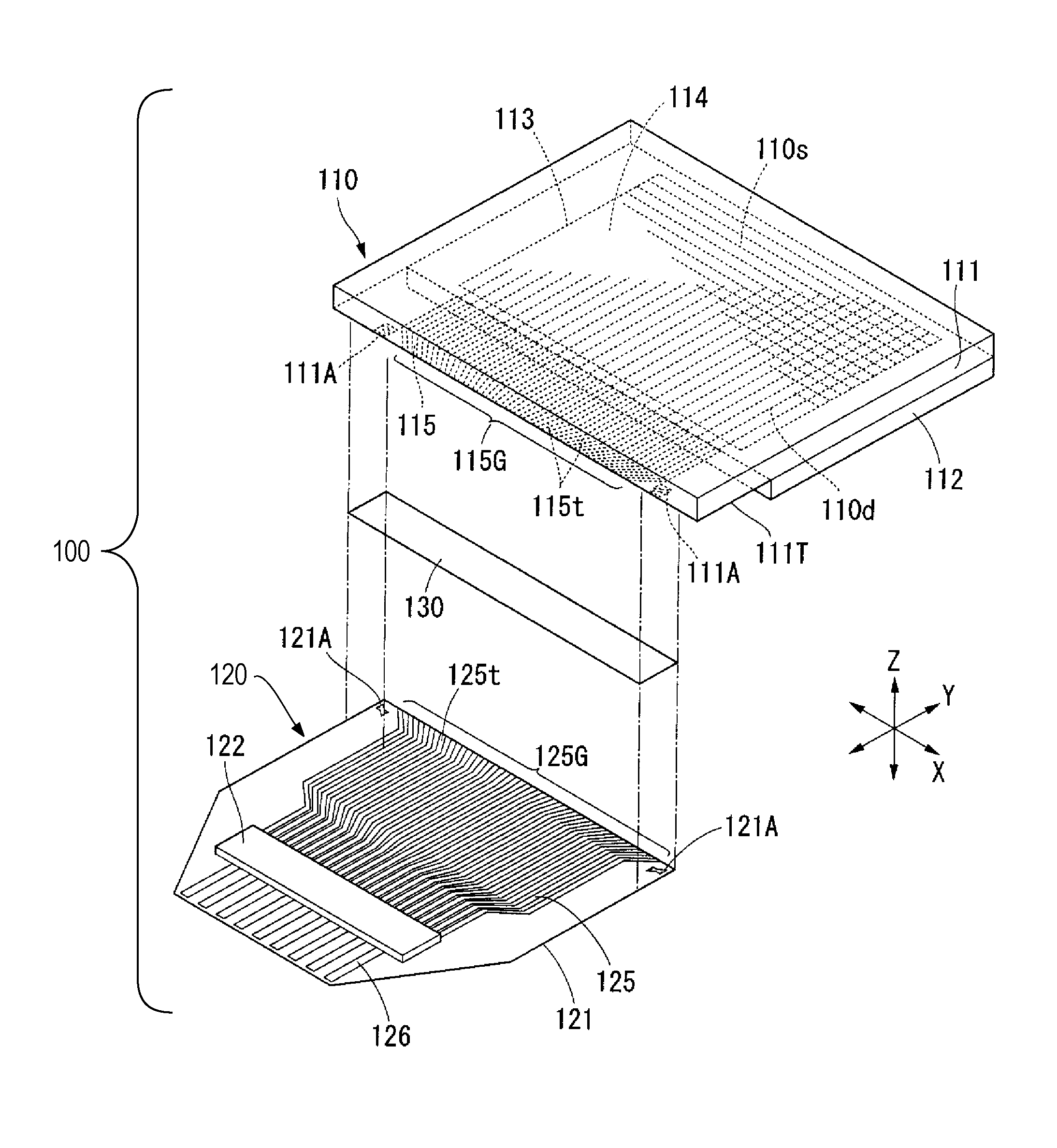
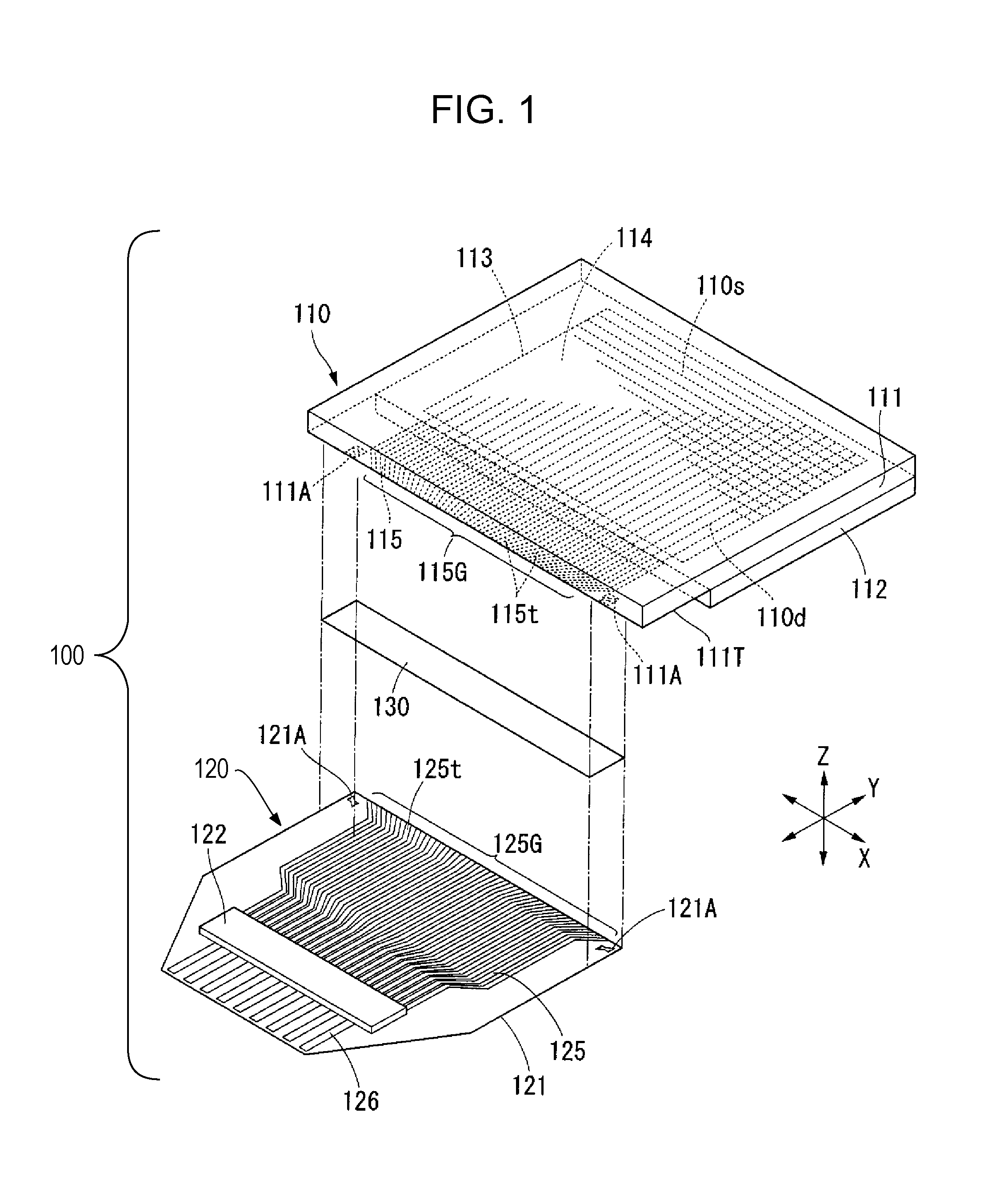
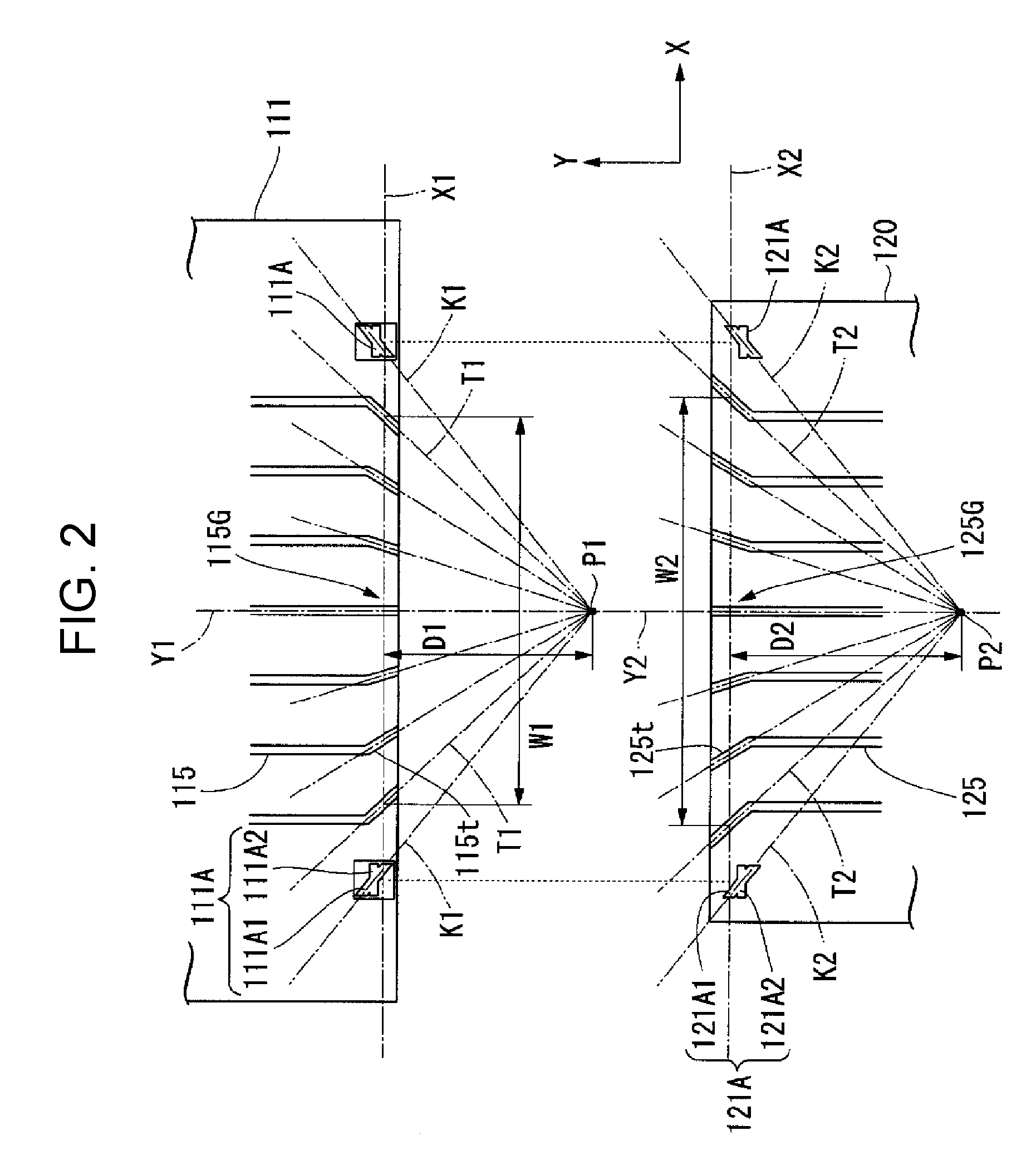
[0038]A preferred embodiment of the present invention will be described with reference to the drawings. However, it is to be understood that the embodiment is for illustrative purposes only and is not to be construed to limit the invention and therefore can be variously modified within the technical spirit and scope of the invention. The scale, the numbers, etc. in the drawings are different from those of the actual structure for the convenience of description.

Structure of Electrooptic Device

[0039]An electrooptic device which is an example of a mount structure equipped with a wiring board according to an embodiment of the invention will be described. FIG. 1 is an exploded perspective view of the electrooptic device according to the embodiment, which is plotted in an XYZ rectangular coordinate system. The positional relationship among the components is illustrated with reference to the XYZ rectangular coordinate system, in which the X axis indicates a specified direction in the horiz...


PUM


Abstract

There is provided a wiring board including: a terminal group including a plurality of terminals arrayed along a specified array axis; and a pair of alignment marks disposed on opposite sides of the terminal group in the direction of the array axis. The alignment marks each have a first portion extending so as to intersect at an angle to the array axis. The first portions of the alignment marks and the plurality of terminals extend from the terminal group to a common phantom center point that is apart from the terminal group in the direction intersecting the array axis.

Description

[0001]The entire disclosure of Japanese Patent Application Nos. 2006-148121, filed May 29, 2006 and 2007-110096, filed Apr. 19, 2007 are expressly incorporated by reference herein.BACKGROUND[0002]1. Technical Field[0003]The present invention relates to a wiring board and a mount structure in which the wiring board is mounted on a mounting object such as an electrooptic panel, for use in personal computers, portable phones, etc. and to a method for manufacturing the mount structure including the step of connecting the terminal groups formed on the components.[0004]2. Related Art[0005]Known electrooptic devices mounted to electronic devices such as portable phones, notebook computers, and TV sets include a structure having an electrooptic panel and a wiring board mounted on the electrooptic panel. When a driving circuit for driving the electrooptic panel is mounted to the panel, the wiring board supplies display data and control signals sent from the display control system of the elec...

Claims


Application Information

Patent Timeline
Patent Type & Authority Applications(United States)
IPC IPC(8): H05K1/00
CPCH05K1/0269H05K1/117H05K3/321H05K2203/166H05K2201/09418H05K2201/09918H05K3/361
Inventor YAMADA, KAZUYUKI
Owner JAPAN DISPLAY WEST
Why Eureka
Try Eureka