Peeling Method

Active Publication Date: 2015-02-12
SEMICON ENERGY LAB CO LTD
View PDF4 Cites 37 Cited by
  • Summary
  • Abstract
  • Description
  • Claims
  • Application Information

AI Technical Summary

Benefits of technology

[0024]According to one embodiment of the present invention, yield in a peeling process can be improved. Moreover, according to one embodiment of the present invention, yield in a manufacturing process of a semiconductor device, a light-emitting device, a display device, an

Problems solved by technology

When a peeling interface deteriorates in peelability in a peeling step, high stress

Method used


Image

  • Peeling Method
  • Peeling Method
  • Peeling Method

Examples


embodiment 1

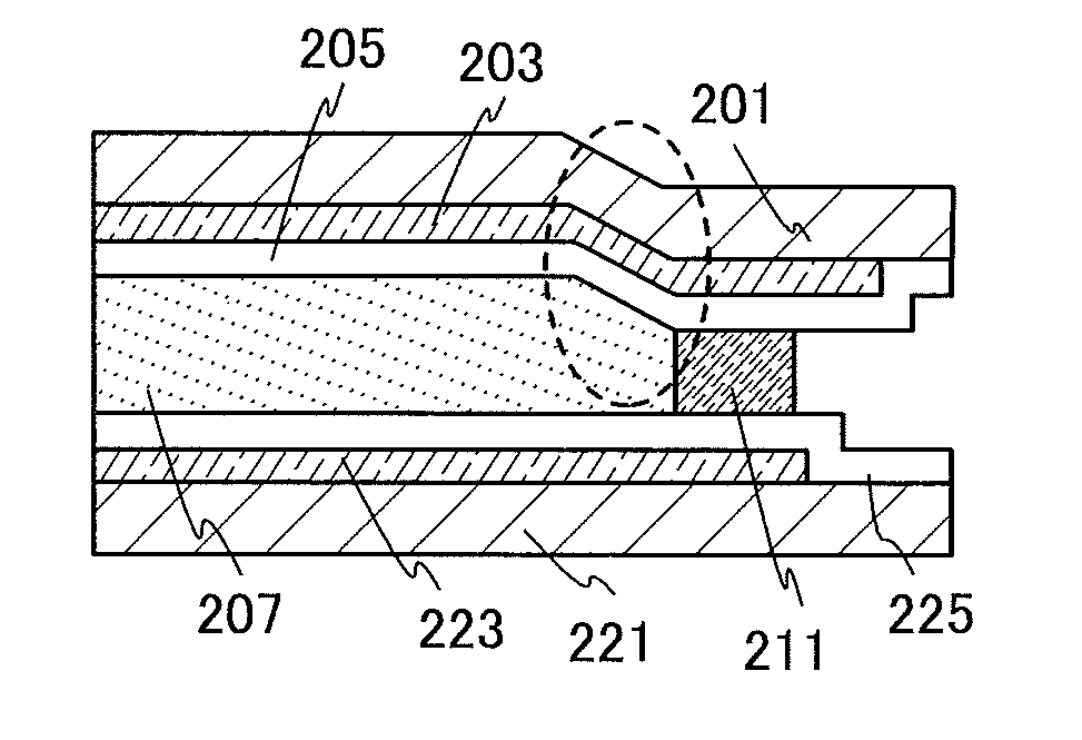
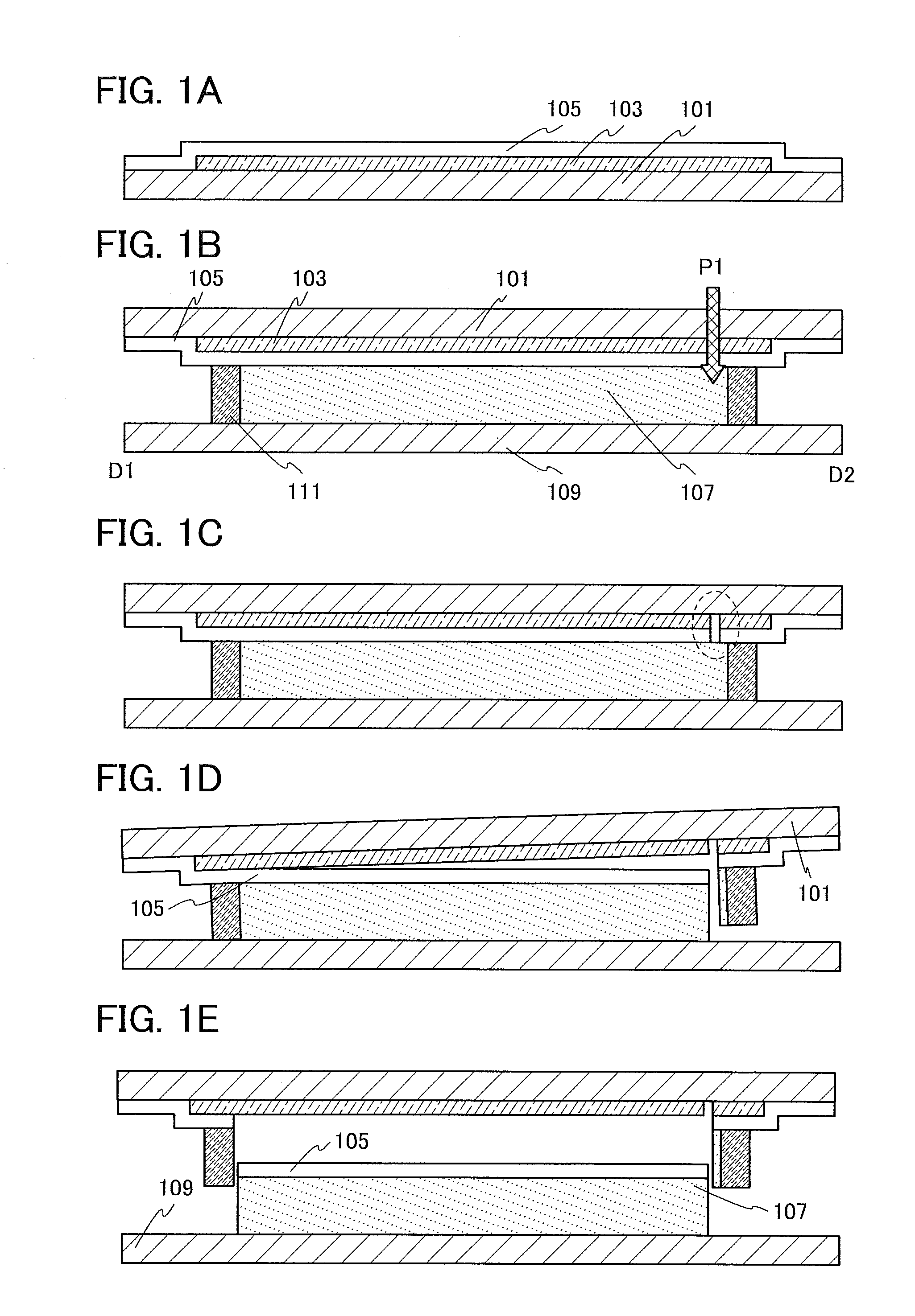
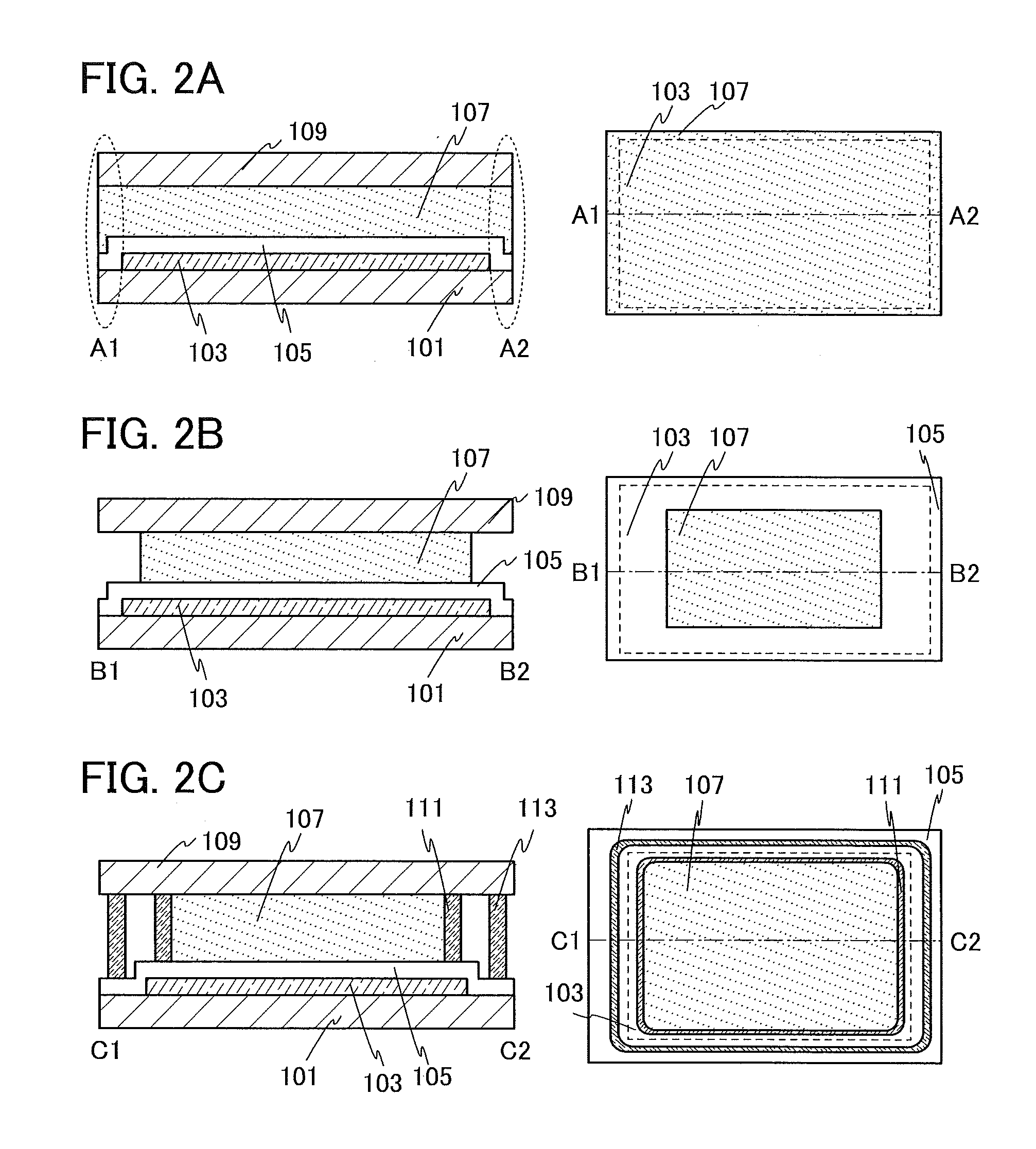
[0067]In this embodiment, the peeling method of one embodiment of the present invention will be described with reference to FIGS. 1A to 1E, FIGS. 2A to 2C, FIG. 3A, FIGS. 3B1 to 3B8, FIG. 3C, FIGS. 4A to 4D, FIGS. 5A to 5D, FIGS. 6A to 6D, FIGS. 7A to 7D, FIGS. 8A to 8D, FIGS. 9A to 9C, and FIGS. 10A to 10I.

[0068]Specifically, one embodiment of the present invention is a peeling method including a first step of forming a peeling layer over a first substrate, a second step of forming a layer to be peeled including a first layer in contact with the peeling layer over the peeling layer, a third step of curing a bonding layer in an overlapping manner with the peeling layer and the layer to be peeled, a fourth step of removing part of the first layer overlapping with the peeling layer and the bonding layer to form a peeling starting point, and a fifth step of separating the peeling layer and the layer to be peeled.

[0069]According to one embodiment of the present invention, in a region wh...

embodiment 2

[0174]In this embodiment, a flexible light-emitting device that can be manufactured according to one embodiment of the present invention and a method for manufacturing the light-emitting device will be described with reference to FIGS. 11A to 11C, FIGS. 12A to 12C, FIGS. 13A to 13C, FIGS. 14A to 14C, FIGS. 15A to 15C, FIGS. 16A to 16C, FIGS. 17A to 17C, FIGS. 18A to 18C, FIGS. 19A and 19B, FIGS. 20A and 20B, FIGS. 21A and 21B, FIGS. 22A and 22B, FIGS. 23A to 23C, FIGS. 24A and 24B, and FIG. 25.

[0175]FIGS. 11A to 11C, FIGS. 12A to 12C, FIGS. 13A to 13C, and FIGS. 14A to 14C illustrate examples of a flexible light-emitting device including an organic EL element as a light-emitting element.

Structural Example 1

[0176]FIG. 11A is a plan view of the light-emitting device, and FIG. 11B is a cross-sectional view taken along dashed-dotted lines X1-Y1 and V1-W1 in FIG. 11A. The light-emitting device illustrated in FIGS. 11A and 11B is a bottom-emission light-emitting device.

[0177]The light-emi...

example 2

Structural Example 2

[0181]FIG. 12A is a plan view of the light-emitting device, and FIG. 12B is a cross-sectional view taken along dashed-dotted line X2-Y2 in FIG. 12A. The light-emitting device illustrated in FIGS. 12A and 12B is a top-emission light-emitting device.

[0182]The light-emitting device in FIG. 12B includes a flexible substrate 420, the bonding layer 422, the insulating layer 424, a conductive layer 408, the insulating layer 405, the organic EL element 450 (the first electrode 401, the EL layer 402, and the second electrode 403), a conductive layer 410, the bonding layer 407, the flexible substrate 428, and a light extraction structure 409. The second electrode 403, the bonding layer 407, the flexible substrate 428, and the light extraction structure 409 transmit visible light.

[0183]The organic EL element 450 is provided over the flexible substrate 420 with the bonding layer 422 and the insulating layer 424 provided therebetween. The organic EL element 450 is sealed with...


PUM


Abstract

To improve the yield in a peeling process and improve the yield in a manufacturing process of a flexible light-emitting device or the like, a peeling method includes a first step of forming a peeling layer over a first substrate, a second step of forming a layer to be peeled including a first layer in contact with the peeling layer over the peeling layer, a third step of curing a bonding layer in an overlapping manner with the peeling layer and the layer to be peeled, a fourth step of removing part of the first layer overlapping with the peeled layer and the bonding layer to form a peeling starting point, and a fifth step of separating the peeling layer and the layer to be peeled. The peeling starting point is preferably formed by laser light irradiation.

Description

BACKGROUND OF THE INVENTION[0001]1. Field of the Invention[0002]The present invention relates to an object, a method, or a manufacturing method. In addition, the present invention relates to a process, a machine, manufacture, or a composition of matter. One embodiment of the present invention relates to a semiconductor device, a light-emitting device, a display device, an electronic device, a lighting device, or a manufacturing method thereof. In particular, one embodiment of the present invention relates to a light-emitting device using an organic electroluminescence (hereinafter also referred to as EL) phenomenon, and a method for manufacturing the light-emitting device. In particular, one embodiment of the present invention relates to a peeling method and a method for manufacturing a device including a peeling process. Moreover, one embodiment of the present invention relates to a laser irradiation system that can be used for the method for manufacturing the device.[0003]2. Descr...

Claims


Application Information

Patent Timeline
IPC IPC(8): H01L51/56H01L51/52H01L51/00
CPCH01L51/56H01L51/524H01L51/0024H10K71/50H10K71/80H10K50/841H10K71/00
Inventor AOYAMA, TOMOYACHIDA, AKIHIROKOMATSU, RYU
Owner SEMICON ENERGY LAB CO LTD
Why Eureka
Try Eureka