Method of forming silicon nitride film and method of manufacturing semiconductor device

a technology of silicon nitride and manufacturing method, which is applied in the direction of semiconductor devices, chemical vapor deposition coatings, coatings, etc., can solve the problems of low deposition rate, inconvenient mass production, and low utilization efficiency of raw material gas, so as to achieve ideal balance of composition ration and eliminate the damage to the gate oxide layer caused by charge-up. , the effect of good step coverag

Active Publication Date: 2009-03-31
ULVAC INC
View PDF29 Cites 77 Cited by
  • Summary
  • Abstract
  • Description
  • Claims
  • Application Information

AI Technical Summary

Benefits of technology

[0012]According to the invention, damage onto the gate oxide layer caused by a charge-up is eliminated because the raw material gas species are decomposed without using plasma. Further, the invention is appropriate to the manufacturing of semiconductor devices with 65-nanometer technology or more recent one because the thin films can be formed at a low temperature as low as 400 degrees centigrade, for example. Furthermore, according to the invention, silicon nitride films having a good step coverage, lower content of hydrogen, ideal balance of composition ration of silicon and nitrogen can be obtained.
[0013]As a result, according to the invention, it becomes possible to manufacture semiconductor devices of a high performance with a high degree of integration, and thus, the industrial merit is great.

Problems solved by technology

However, use of the plasma CVD method involves some problems such as plasma charge-up of the wafer, leaving room for improvement in recent ultrafine semiconductor devices as typified by the 65-nm node generation.
However, it has a low deposition rate because of low decomposition rate of raw material gas, and hence there is a problem that it is not suitable to mass production.
Furthermore, in the conventional plasma CVD method, the usage efficiency of raw material gas is only a few percent.
If the pressure during deposition is decreased and the feed rate for ammonia relative to silane is decreased, the coverage is improved, but a silicon-rich thin film is formed because of insufficient nitridation of silicon.

Method used


Image

  • Method of forming silicon nitride film and method of manufacturing semiconductor device
  • Method of forming silicon nitride film and method of manufacturing semiconductor device
  • Method of forming silicon nitride film and method of manufacturing semiconductor device

Examples


Embodiment Construction

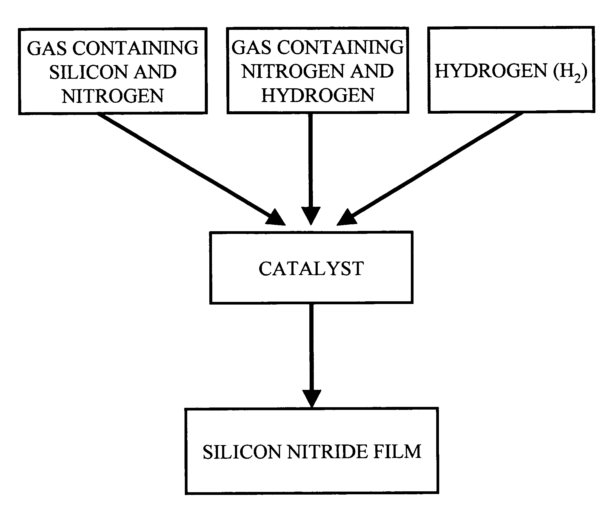
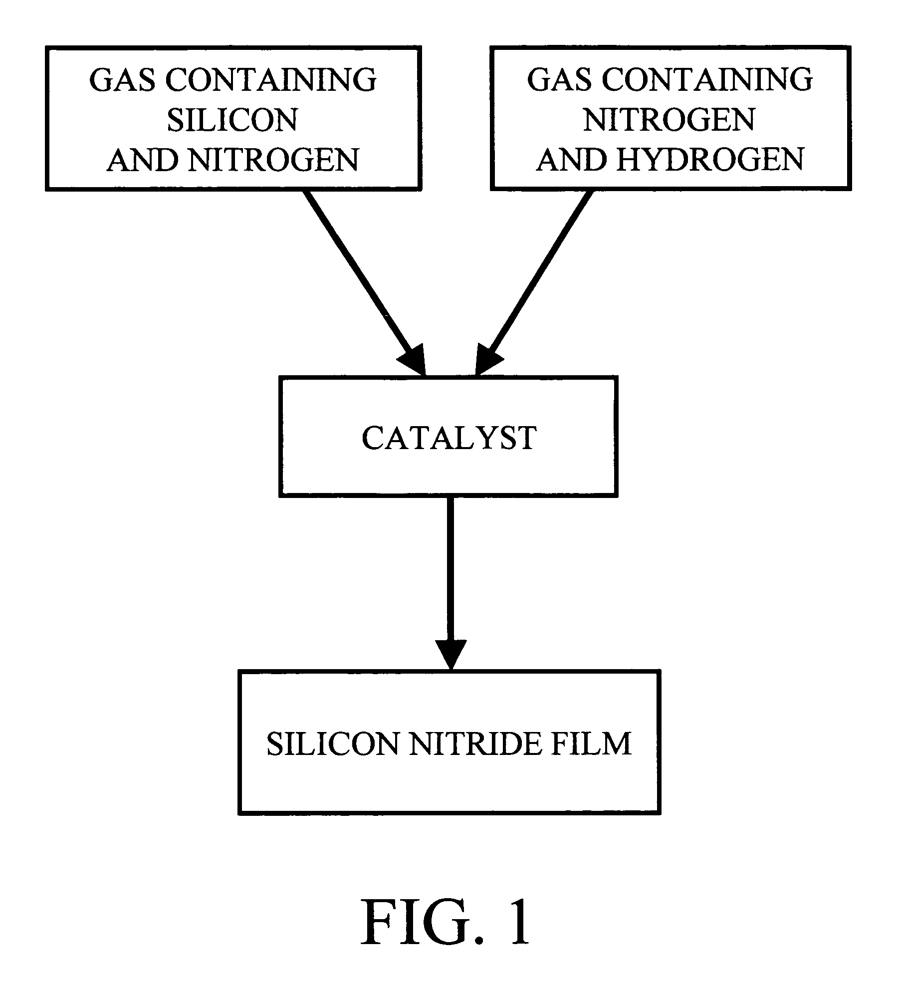
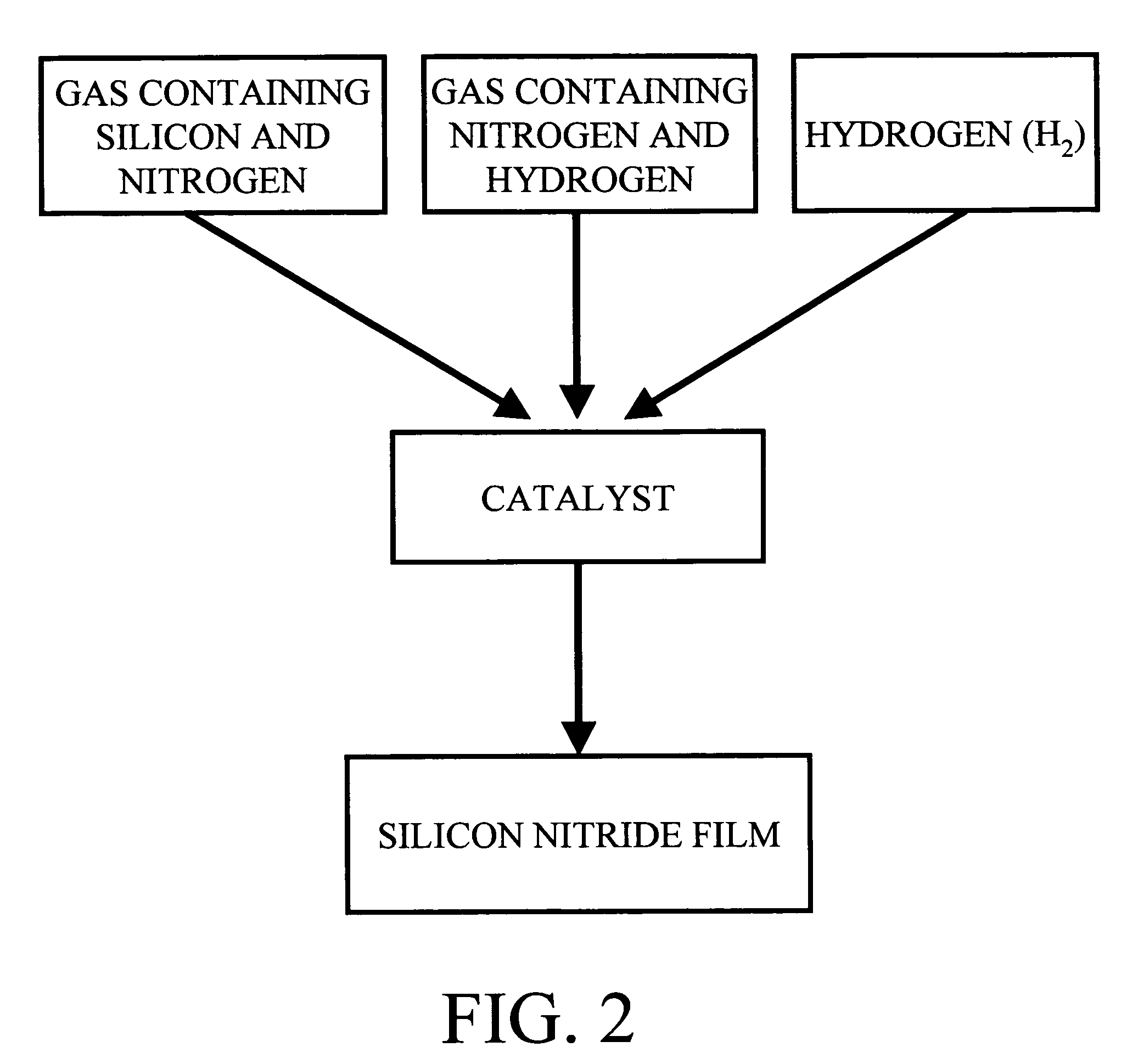
[0030]The catalytic CVD method employed in the invention has the following essential advantages compared to the photo-CVD disclosed, for example, in Japanese Laid-Open Patent Application S61-234534 (1986):

[0031]First, by using the catalytic CVD method, thin films having higher density and higher purity can be obtained than by using the photo-CVD method at a same deposition temperature. For example, in the case where hydride row materials such as silane-group or amine-group are used, the amount of hydrogen incorporated in the thin film can be greatly reduced by using the catalytic CVD method.

[0032]In the case of the photo-CVD including a laser-assisted CVD, the optimum pressure for film deposition is in a range of 100 pascals through a few hundreds pascals, which is similar to the conventional low pressure CVD and plasma CVD. This optimum range is determined by the fact that practical and / or productive deposition rate is not obtained if the pressure is set lower than the range becaus...


PUM

PropertyMeasurementUnit
temperatureaaaaaaaaaa

Abstract

A method of forming a silicon nitride film comprises: forming a silicon nitride film by applying first gas containing silicon and nitrogen and second gas containing nitrogen and hydrogen to catalyst heated in a reduced pressure atmosphere. A method of manufacturing a semiconductor device comprising the steps of: forming a silicon nitride film by the method as claimed in claim 1 on a substrate having the semiconductor layer, a gate insulation film selectively provided on a principal surface of the semiconductor layer, and a gate electrode provided on the gate insulation film; and removing the silicon nitride film on the semiconductor layer and the gate electrode and leaving a sidewall comprising the silicon nitride film on a side surface of the gate insulation film and the gate electrode by etching the silicon nitride film in a direction generally normal to the principal surface of the semiconductor layer. A method of manufacturing a semiconductor device comprising the steps of: forming a silicon nitride film by the method as claimed in claim 1 on a substrate including a semiconductor layer; forming an interlayer insulation layer on the silicon nitride film; forming a layer having an opening on the interlayer insulation layer; and etching the interlayer insulation layer via the opening in a condition where an etching rate for the silicon nitride film is greater than an etching rate for the interlayer insulation layer.

Description

CROSS-REFERNCE TO ERLATED APPLICATIONS[0001]This Application is based upon and claims the benefit of priority from the prior Japanese Patent Application No. 2004-058214, filed on Mar. 2, 2004; the entire contents of which are incorporated herein by reference.BACKGROUND OF THE INVENTION[0002]The invention relates to a method of forming a silicon nitride film and a method of manufacturing a semiconductor device, and more particularly, to a method of forming a silicon nitride film having good step coverage by the catalytic CVD method and a method of manufacturing a semiconductor device.[0003]Silicon nitride film plays an important role in various applications such as passivation film, etching stopper, and hard mask in semiconductor devices. Furthermore, it is used as gate sidewall for forming LDD (lightly doped drain) structure of MOSFET (metal-oxide-semiconductor field effect transistor).[0004]Conventionally, silicon nitride film used for these applications is formed by the plasma CVD...

Claims


Application Information

Patent Timeline
Patent Type & Authority Patents(United States)
IPC IPC(8): H01L21/4763H01L29/78H01L21/318
CPCC23C16/045C23C16/345C23C16/44H01L21/0217H01L21/02277H01L21/31116H01L21/31144H01L21/3212H01L21/76802H01L21/76829H01L21/76831H01L21/76834H01L29/7833
Inventor SAITO, TSUYOSHIITOH, HIROMIKITAZOE, MAKIKO
Owner ULVAC INC
Why Eureka
Try Eureka