Method for depositing thin tungsten film with low resistivity and robust micro-adhesion characteristics

a technology of microadhesion and thin tungsten, which is applied in the direction of liquid surface applicators, chemical vapor deposition coatings, coatings, etc., can solve the problems of inability to produce easily and reliably, and achieve good adhesion to the underlying layer, good uniformity, and low resistivity

Inactive Publication Date: 2011-11-15
NOVELLUS SYSTEMS
View PDF93 Cites 93 Cited by
  • Summary
  • Abstract
  • Description
  • Claims
  • Application Information

AI Technical Summary

Benefits of technology

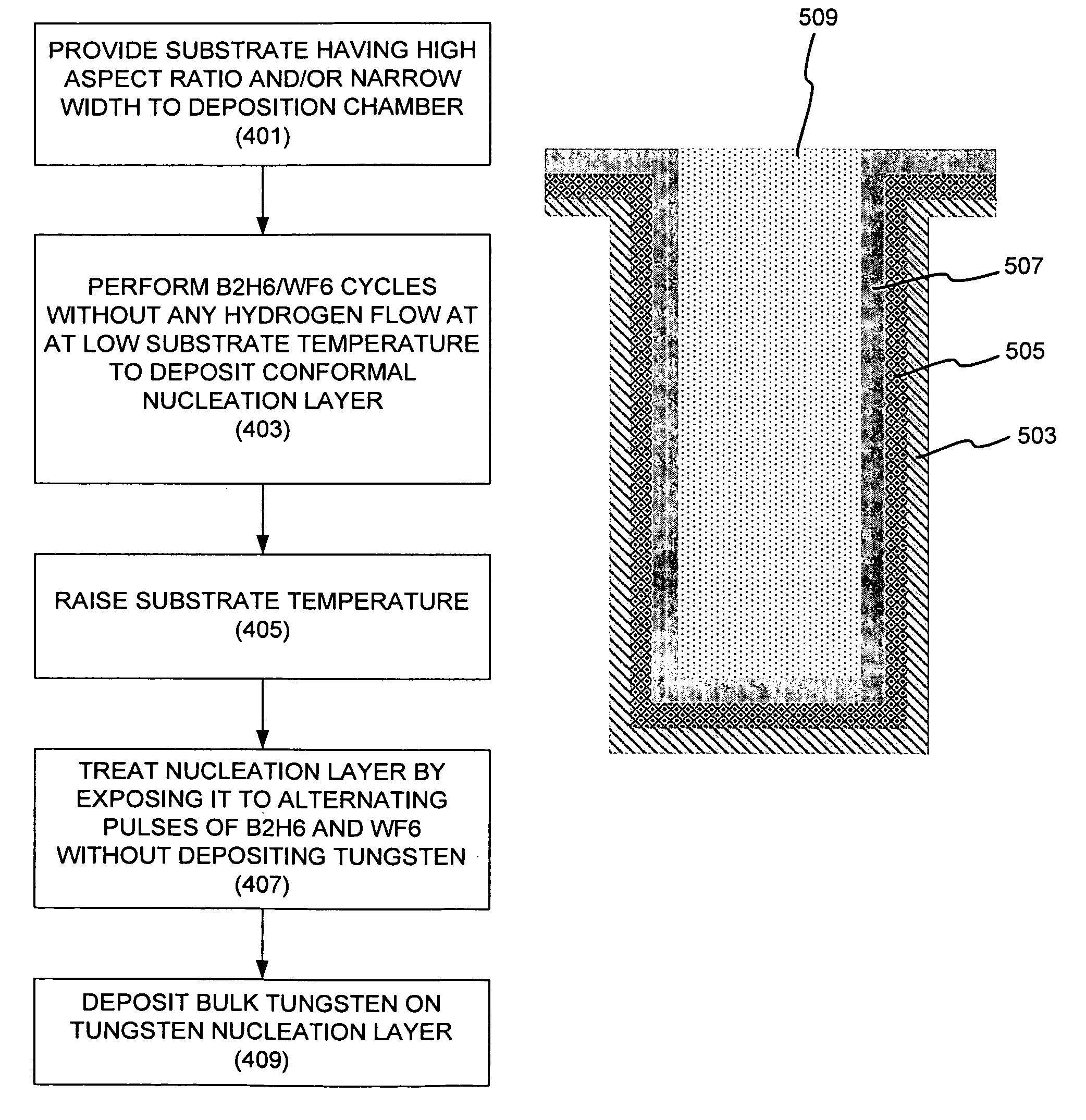
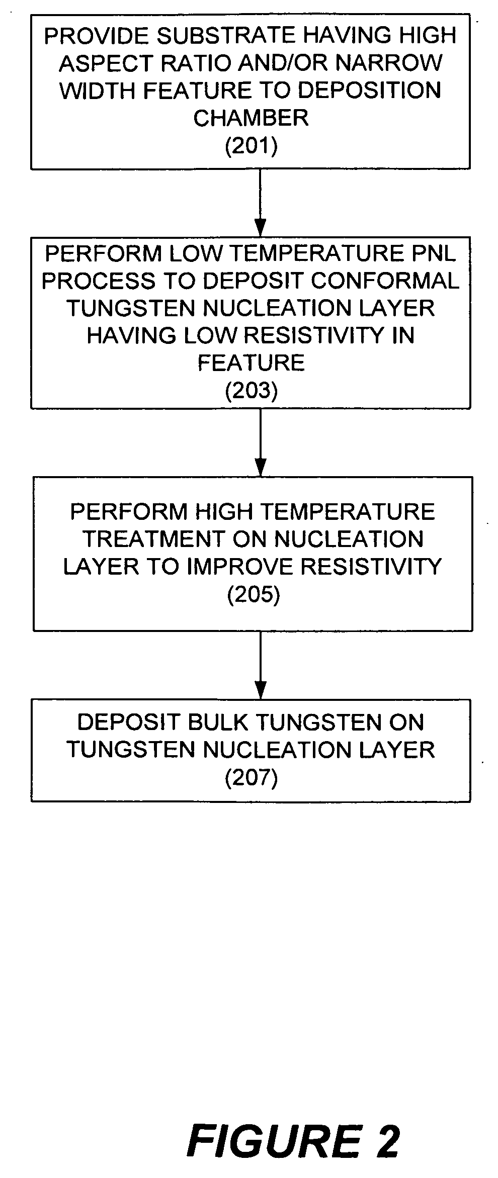
[0004]Methods of forming low resistivity tungsten films with good uniformity and good adhesion to the underlying layer are provided. The methods involve forming a tungsten nucleation layer using a pulsed nucleation layer process at low temperature and then treating the deposited nucleation layer prior to depositing the bulk tungsten fill. The treatment operation lowers resistivity of the deposited tungsten film. In certain embodiments, depositing the nucleation layer involves a boron-based chemistry in the absence of hydrogen. Also in certain embodiments, the treatment operations involve exposing the nucleation layer to alternating cycles of a reducing agent and a tungsten-containing precursor. The methods are useful for depositing films in high aspect ratio and / or narrow features. The films exhibit low resistivity at narrow line widths and excellent step coverage.

Problems solved by technology

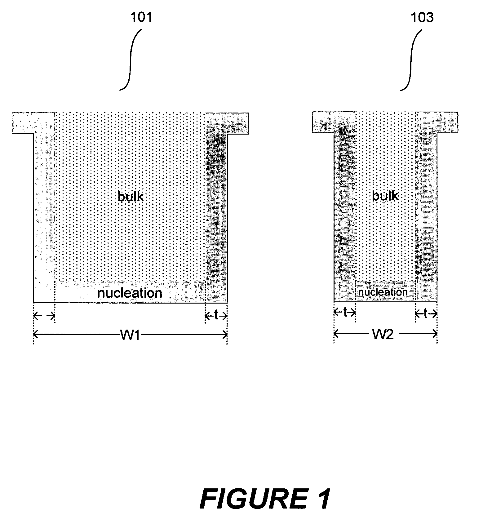
The tungsten bulk layer is generally deposited more rapidly than the nucleation layer, but cannot be produced easily and reliably without first forming the nucleation layer.

Method used


Image

  • Method for depositing thin tungsten film with low resistivity and robust micro-adhesion characteristics
  • Method for depositing thin tungsten film with low resistivity and robust micro-adhesion characteristics
  • Method for depositing thin tungsten film with low resistivity and robust micro-adhesion characteristics

Examples


example 1

[0039]A W nucleation layer was formed in features having an AR of 8.5:1 and a top opening was 0.14 μm at 300° C. using tungsten nucleation layer deposition sequences shown in the table below. Nucleation layers of about 42 Å for process A, 25 Å for process C and 35 Å for process B were deposited. Treatment operations were then performed using sequences shown below at 395° C. (Note that for process A, the ‘treatment’ involved a B2H6 / WF6 cycle having longer pulse duration; tungsten film was deposited during this step.) Note that process is in accordance with the embodiments depicted in FIG. 4a. A bulk tungsten layer was then deposited on each nucleation layer. Resistivity at 600 Angstroms and resistance non-uniformity at 3 mm edge exclusion were measured. The films were also examined for areas of micro-peeling. Process conditions and results are shown below in Table 1

[0040]

TABLE 1ResistivityatNucleation600LayerAngstromsMicro-DepositionTreatment(μΩ-4 mm EEpeelingProcessSequenceSequencec...

example 2

[0041]A W nucleation layer was formed on semiconductor substrates (planar) at 300° C. using tungsten nucleation layer deposition sequences shown in the table below. Nucleation layer thicknesses of about 35 Å for Process D, about 25 Å for processes E and F were deposited. Process D used a single B2H6 / WF6 cycles followed by three SiH4 / WF6 cycles in the presence of H2; processes E and F used a low resistivity tungsten deposition process without any hydrogen. Low resistivity treatment operations were then performed using 5 cycles of the sequences shown below at 395° C. Process D used pulses of B2H6 (no intervening pulses); processes E and F both used alternating B2H6 and WF6 pulses. Processes E and F were performed in accordance with the embodiments depicted in FIG. 4a. A bulk tungsten layer was then deposited on each nucleation layer. Resistivity at 600 Angstroms and resistance non-uniformity at 4 mm edge exclusion were measured. For each process, conditions were optimized to minimize ...

example 3

[0043]Similarly, when tuned for low resistivity, processes as shown in FIG. 4a result in lower particle counts and micro-peeling for similar resistivities:

[0044]

TABLE 3NucleationTreatment - 5 cyclesResistivityLayerB2H6WF6atMicro-Depositionflowrate / flowrate / 600 ÅpeelingProcessSequencepulse timepulse time(μΩ-cm)observed?G1 B2H6 / WF6350 sccm / 0 / 09.83Yescycle + 31 secSH4 / WF6cycles (inpresence ofH2)H5 B2H6 / WF6250 sccm / 0 / 09.76No orcycles (no1 secreduced**H2)**For particular split shown here, micropeeling was not measured; however from other experiments, it was shown that Process H results in no or reduced micropeeling compared to Process G.


PUM

PropertyMeasurementUnit
temperatureaaaaaaaaaa

Abstract

Methods of forming low resistivity tungsten films with good uniformity and good adhesion to the underlying layer are provided. The methods involve forming a tungsten nucleation layer using a pulsed nucleation layer process at low temperature and then treating the deposited nucleation layer prior to depositing the bulk tungsten fill. The treatment operation lowers resistivity of the deposited tungsten film. In certain embodiments, the depositing the nucleation layer involves a boron-based chemistry in the absence of hydrogen. Also in certain embodiments, the treatment operations involve exposing the nucleation layer to alternating cycles of a reducing agent and a tungsten-containing precursor. The methods are useful for depositing films in high aspect ratio and / or narrow features. The films exhibit low resistivity at narrow line widths and excellent step coverage.

Description

CROSS-REFERENCE TO RELATED APPLICATION[0001]This application claims benefit under 35 U.S.C. 119(e) of U.S. Provisional Application No. 61 / 061,078, filed Jun. 12, 2008. This application is incorporated by reference herein in its entireties and for all purposes.FIELD OF INVENTION[0002]This invention relates to methods for preparing tungsten films. Embodiments of the invention are useful for integrated circuit applications that require thin tungsten films having low electrical resistivity with good uniformity and good adhesion.BACKGROUND[0003]The deposition of tungsten films using chemical vapor deposition (CVD) techniques is an integral part of many semiconductor fabrication processes. Tungsten films may be used as low resistivity electrical connections in the form of horizontal interconnects, vias between adjacent metal layers, and contacts between a first metal layer and the devices on the silicon substrate. In a conventional tungsten deposition process, the wafer is heated to the p...

Claims


Application Information

Patent Timeline
Patent Type & Authority Patents(United States)
IPC IPC(8): H01L21/44
CPCC23C16/0281C23C16/045C23C16/14C23C16/45534H01L21/28556H01L21/28562H01L21/76864H01L21/76876H01L21/76877
Inventor CHANDRASHEKAR, ANANDGLASS, MIRKOHUMAYUN, RAASHINADANEK, MICHAELASHTIANI, KAIHANCHEN, FENGCHAN, LANA HIULUIMANE, ANIL
Owner NOVELLUS SYSTEMS
Why Eureka
Try Eureka