Shower head of a wafer treatment apparatus having a gap controller

a technology of wafer treatment and shower head, which is applied in the direction of coating, chemical vapor deposition coating, metallic material coating process, etc., can solve the problems of inability to achieve uniform etching over the entire wafer surface, and inability to achieve uniform etching rate. optimum

Inactive Publication Date: 2005-07-07
SAMSUNG ELECTRONICS CO LTD
View PDF30 Cites 385 Cited by
  • Summary
  • Abstract
  • Description
  • Claims
  • Application Information

AI Technical Summary

Benefits of technology

[0008] In an effort to solve the above problems, it is a feature of an embodiment of the present invention to provide a shower head capable of controlling the distribution amount of a reactant gas depending on a position on a wafer in order to obtain optimum uniformity in etch rate over the entire wafer surface during a fabrication process for a semiconductor device.
[0009] It is another feature of an embodiment of the present invention to provide a shower head capable of controlling the amount of a reactant gas supplied depending on a position on a wafer as desired by compensating for degradation of etch rate uniformity which may occur depending on the position on the wafer during an etch step so that a final etch rate uniformity may be optimized.
[0013] The gap controller preferably determines the position of the first baffle plate to increase the width of the first gap so that the amount of the reactant gas flowing through the plurality of second through holes is increased.
[0032] Each of the plurality of piezoelectric elements may control the amount of the reactant gas flowing from the through holes of the first baffle plate into the gap using a thickness expansion rate of the piezoelectric element adjusted according to the level of voltage applied from the power supply unit. Also, each of the plurality of piezoelectric elements may selectively open or close the plurality of through holes using a thickness expansion rate of the piezoelectric element adjusted according to the level of voltage applied from the supply unit.
[0038] In a shower head according to a fourth aspect of the present invention, a circular first baffle plate has a plurality of through holes. A circular second baffle plate, having a plurality of through holes, is disposed below the first baffle plate with a gap having a predetermined width interposed between the first and second baffle plates. A plurality of piezoelectric elements are disposed between the first and second baffle plates for controlling the amount of a reactant gas flowing through the plurality of through holes formed in the first baffle plate.
[0044] According to the present invention, the width of the gap is selectively decreased or increased by the gap controller, thereby adjusting the amount of reactant gas supplied in accordance with a position on a wafer in a process region of a reaction chamber and making the amount of the reactant gas supplied to a position on the wafer even or uneven depending on the type of application. Thus, according to the present invention, it is easier to adjust the distribution of the reactant gas depending on a position on the wafer in order to obtain optimized etch rate uniformity over the entire wafer surface during the fabrication process of a semiconductor device. Furthermore, the present invention makes it possible to freely adjust the amount of reactant gas supplied, thereby compensating in advance for degradation in etch rate uniformity that may partially occur on the wafer during an etch step.

Problems solved by technology

Thus, the configuration of the conventional shower head involves limitations in developing a new process.
Furthermore, development of a new etching apparatus usually requires numerous simulation processes and significant expense.
For example, in the case of an etch process for forming a gate electrode on a wafer, it may not be desirable to obtain etching uniformity over the entire wafer surface during an etch process step for forming an etch mask layer before gate patterning.
However, in the conventional shower head in which the respective positions of the through holes provided in each baffle and the gap between the baffles are fixed, it is impossible to supply different amounts of gas to different positions on the wafer, thereby increasing the difficulty to optimize the uniformity of a pattern to be formed over the entire wafer surface.
Problems associated with an unevenness in an etch rate during an etch process during a fabrication process for a semiconductor device adversely affect the performance of the device and yields.

Method used


Image

  • Shower head of a wafer treatment apparatus having a gap controller
  • Shower head of a wafer treatment apparatus having a gap controller
  • Shower head of a wafer treatment apparatus having a gap controller

Examples


third embodiment

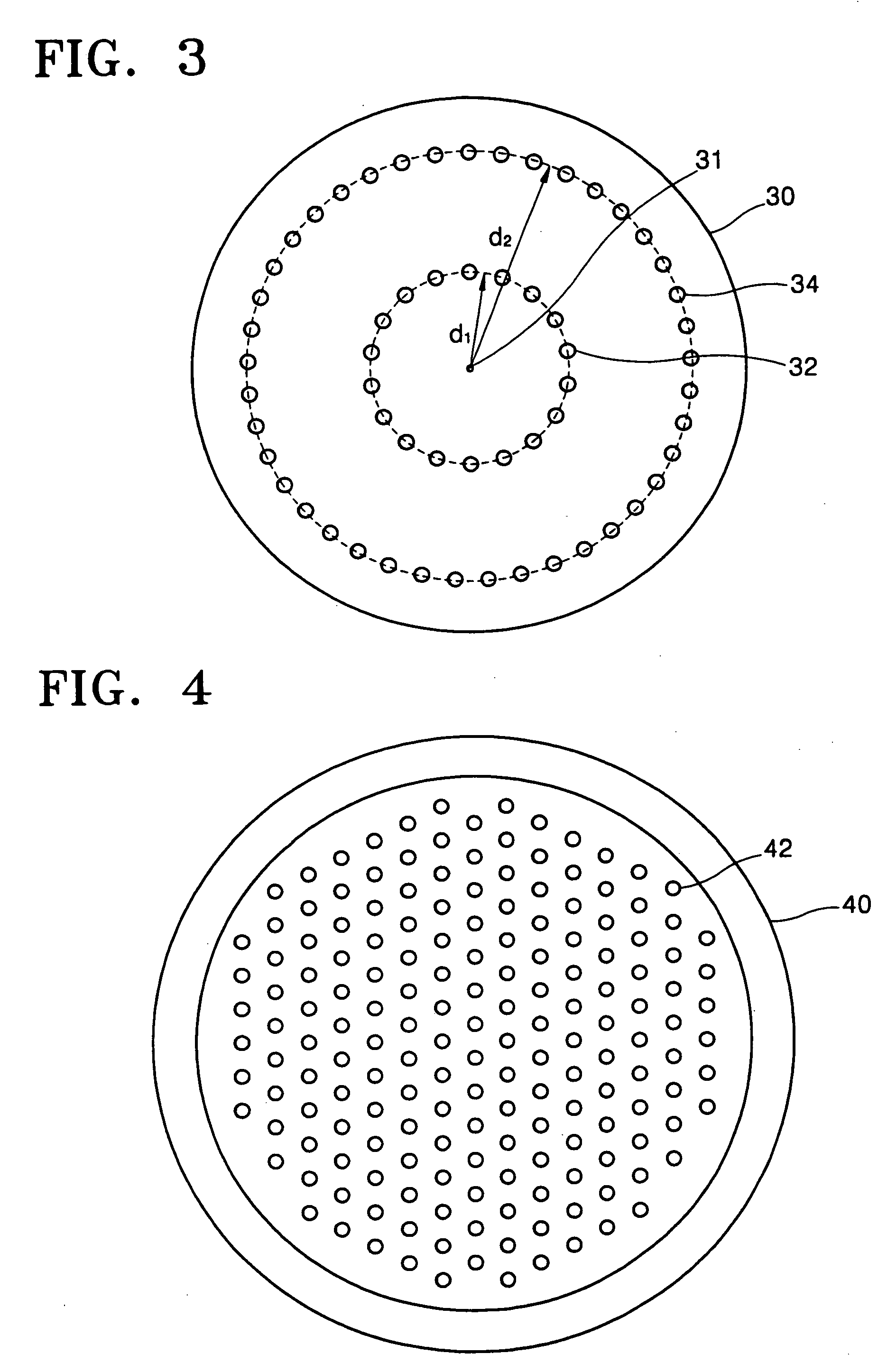
[0099]FIGS. 16A-16C schematically illustrates a configuration of main parts of a shower head according to the present invention. Referring to FIG. 16A, an elevating mechanism 392 and a rotating mechanism 394 are used as a gap controller for determining the first and second gaps 70 and 80. Parts of the shower head in this embodiment other than the elevating mechanism 392 and the rotating mechanism 394 have the same configuration as described in the above embodiments. The elevating mechanism 392 drives the first baffle plate 30 upwardly or downwardly using a first stepping motor 312 in order to determine the width of the second gap 80. The rotating mechanism 394 drives the guide baffle plate 50 upwardly or downwardly by means of a gear drive using the second stepping motor 314.

[0100] The elevating mechanism 392 is integrated with the rotating mechanism 394 as shown in FIG. 16A. The elevating mechanism 392 is movable up or down by power transmitted from the first stepping motor 312. Th...

fourth embodiment

[0107]FIG. 17 schematically illustrates a configuration of main parts of a shower head according to the present invention. In FIG. 17, the same elements are denoted by the same reference numerals, and a detailed explanation thereof will be omitted.

[0108] In the embodiment shown in FIG. 17, a first baffle plate 430 is in contact with a second baffle plate 440. Thus, the width of the second gap 80 disposed between the first and second baffle plates 430 and 440 is effectively zero. A driving shaft 480 for simultaneously driving the first and second baffle plates 430 and 440 upwardly or downwardly is disposed in order to determine the width of the first gap 70 formed between the guide baffle plate 50 and the first baffle plate 430. When the second baffle plate 440 is driven by the driving shaft 480 upwardly or downwardly, the first baffle plate 430 is moved upwardly or downwardly to follow the upward or downward movement of the second baffle plate 440, thereby limiting the width of the ...

fifth embodiment

[0120]FIG. 21 illustrates a cross-sectional view for explaining the configuration of main parts of a shower head according to the present invention. In FIG. 21, the same elements are denoted by the same reference numerals, and a detailed explanation thereof will be omitted.

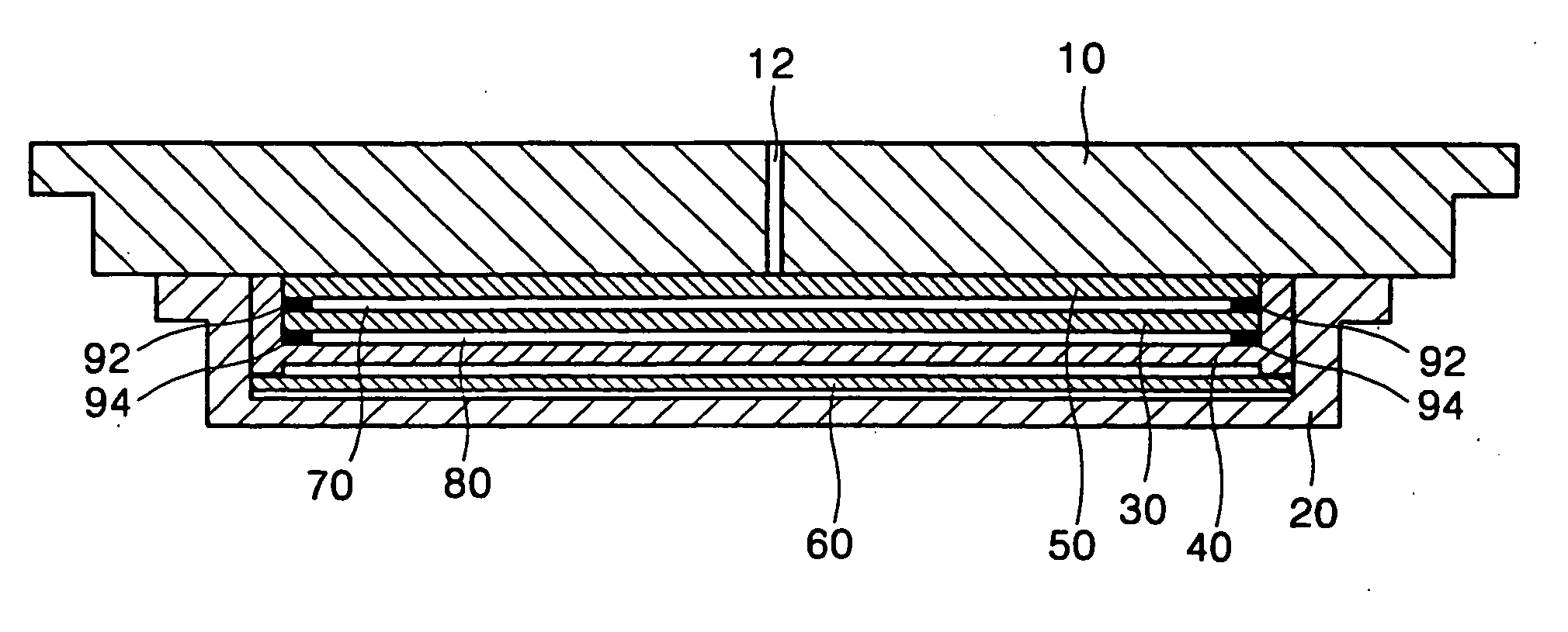
[0121] Similar to the first embodiment shown in FIG. 1, the shower head according to the fifth embodiment shown in FIG. 21 includes a first baffle plate 530 disposed between the top plate 10 and the face plate 20 and a second baffle plate 540 disposed between the first baffle plate 530 and the face plate 20. The second baffle plate 540 has a top surface that limits the second gap 80 for forming a flow passage of the reactant gas between the first and second baffle plates 530 and 540. In order to control the amount of the reactant gas through the second gap 80 formed between the first and second baffle plates 530 and 540, a plurality of piezoelectric elements 582, 584, and 586 are disposed on the top surface of the...


PUM

PropertyMeasurementUnit
voltageaaaaaaaaaa
thicknessaaaaaaaaaa
piezoelectricaaaaaaaaaa

Abstract

A shower head for adjusting distribution of a reactant gas in a process region of a semiconductor manufacturing reaction chamber, wherein a top plate has a gas port for introducing the reactant gas into the reaction chamber; a face plate, having through holes, disposed opposite the process region; a first baffle plate, having through holes, disposed between the top plate and the face plate and capable of moving up or down, wherein the first baffle plate has a top surface that defines a first gap for forming a first lateral flow passage; a second baffle plate, having through holes, disposed between the first baffle plate and the face plate and capable of moving up or down, wherein the second baffle plate has a top surface that defines a second gap for forming a second lateral flow passage; and a gap controller for determining widths of the first and second gaps.

Description

BACKGROUND OF-THE INVENTION [0001] 1. Field of the Invention [0002] The present invention relates to an apparatus for manufacturing a semiconductor device. More particularly, the present invention relates to a shower head provided to supply a reactant gas using plasma to a reaction chamber in a wafer treatment apparatus. [0003] 2. Description of the Related Art [0004] As the integration density of semiconductor devices increases, a design rule decreases and the diameter of a wafer increases. Large wafers often undergo multiple steps for fabricating semiconductor devices, including, for example, deposition processes for depositing material layers on a wafer or etch processes for etching material layers on the wafer in a predetermined pattern by supplying a reactant gas from the upper portion of a reaction chamber for depositing or etching the wafer. In particular, as wafer sizes increase, during etch processes, it is important to optimize uniformity in etch rates over the entire wafe...

Claims


Application Information

Patent Timeline
Patent Type & Authority Applications(United States)
IPC IPC(8): H01L21/3065C23C16/44C23C16/455H01L21/00
CPCC23C16/45565H01L21/67017C23C16/45589H01L21/3065
Inventor PARK, JONG-CHULKIM, DONG-HYUNKWON, O-IKJO, HYE-JIN
Owner SAMSUNG ELECTRONICS CO LTD
Why Eureka
Try Eureka