Method of manufacturing semiconductor device

a manufacturing method and semiconductor technology, applied in the direction of semiconductor devices, basic electric elements, electrical appliances, etc., can solve the problems of inability to ensure the processing accuracy of sidewall spacers, inability to have vertical profiles of sidewall spacers, tapered sidewall spacers,

Inactive Publication Date: 2006-03-16
KK TOSHIBA
View PDF6 Cites 423 Cited by
  • Summary
  • Abstract
  • Description
  • Claims
  • Application Information

AI Technical Summary

Problems solved by technology

As the dimensions of semiconductor devices are scaled down, it has become increasingly difficult to ensure the processing accuracy of sidewall spacers.
However, increasing the carbon-to-fluorine ratio results in a tapered sidewall spacer with the base widened; that is, the sidewall spacer fails to have vertical profile.
Thus, if the sidewall spacer is formed by means of plasma etching using a gas containing fluorine such as a fluorocarbon-based gas, it is difficult to provide high etch selectivity of spacer insulating film to silicon substrate and to form a sidewall spacer vertical in profile.
For this reason, it is difficult to obtain a sidewall spacer in a desired processed state.
In addition, as the dimensions of semiconductor devices are scaled down, it has become increasingly difficult to obtain via holes and contact holes in desired processed states.
The presence of fluorine or hydrofluoric acid results in the occurrence...

Method used


Image

  • Method of manufacturing semiconductor device
  • Method of manufacturing semiconductor device
  • Method of manufacturing semiconductor device

Examples


embodiment 1

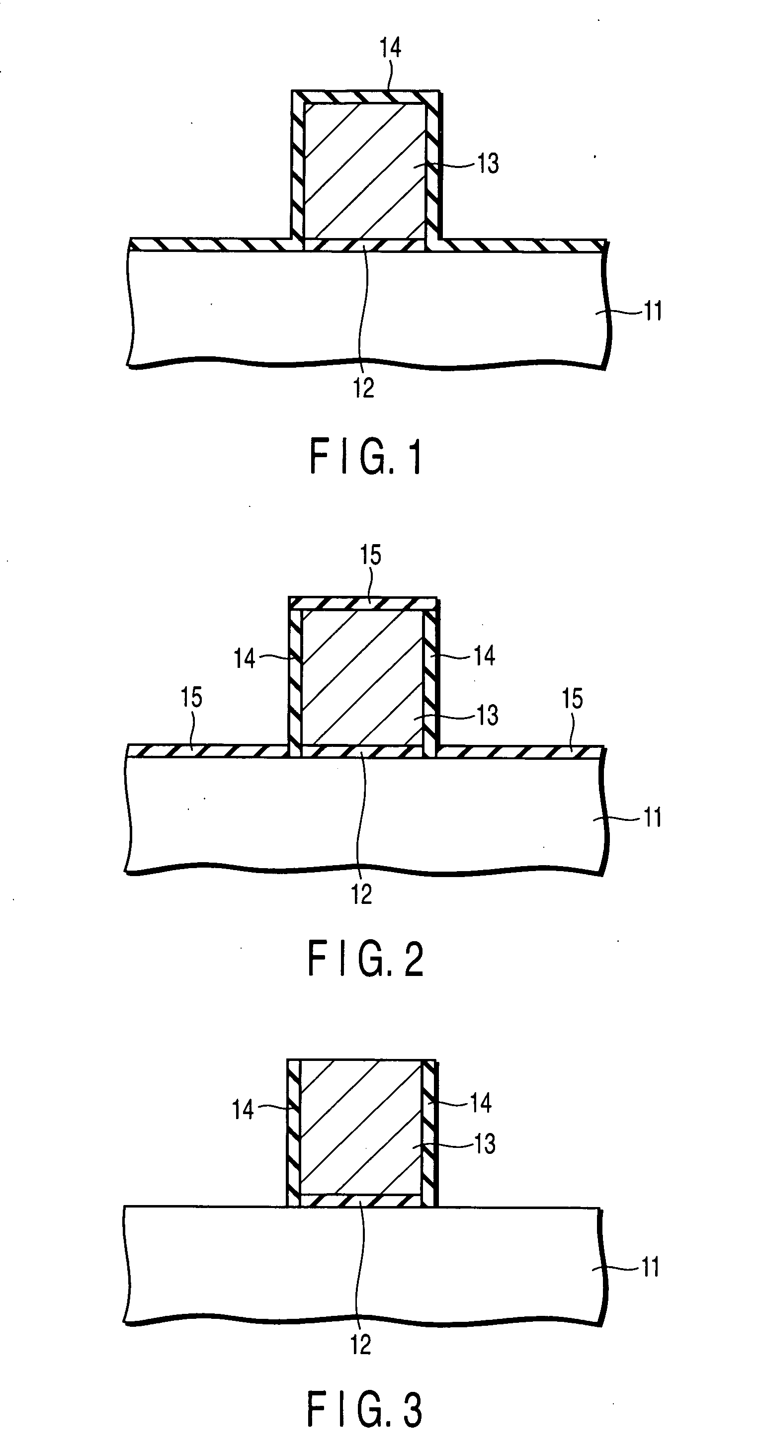
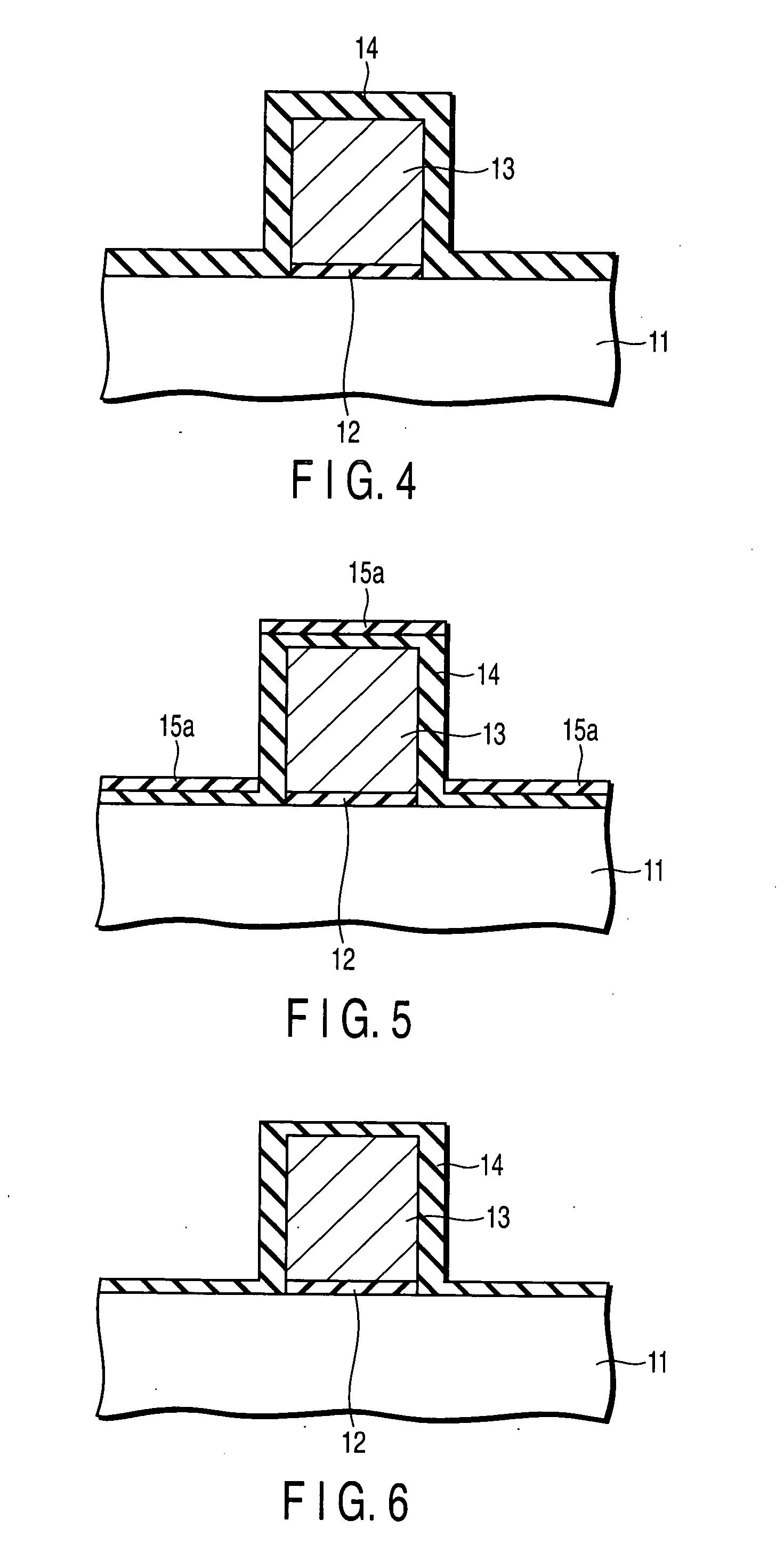
[0024] A semiconductor device manufacturing method according to a first embodiment of the invention will be described with reference to sectional views shown in FIGS. 1, 2 and 3.

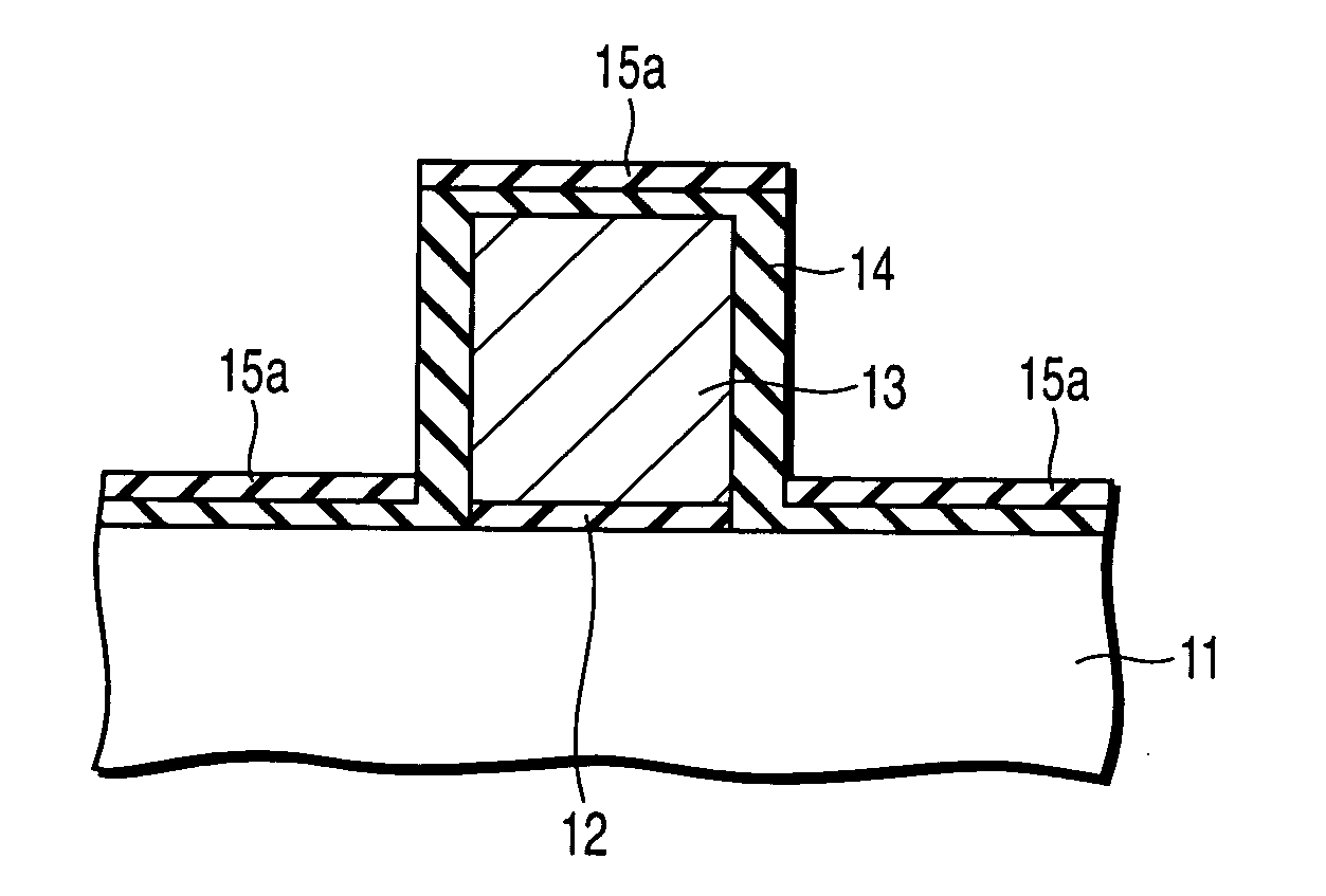
[0025] First, as shown in FIG. 1, a silicon substrate (semiconductor substrate) 11 is formed on top with a gate insulating film 12 and a gate electrode (gate interconnect line) 13 is formed on the gate insulating film as a gate structure. The gate insulating film 12 is formed of silicon oxide and the gate electrode 13 is formed of polysilicon. Although the gate insulating film 12 is shown here processed into the shape of gate together with the gate electrode 13, it may be left unprocessed to cover the entire major surface of the silicon substrate 11. Subsequently, a spacer insulating film (first insulating film) 14 having a thickness of 10 nm and formed of silicon nitride is formed so as to cover the surface (top and side surfaces) of the gate electrode 13 and the surface (major surface) of the silicon subs...

embodiment 2

[0030] A semiconductor device manufacturing method according to a second embodiment of the invention will be described with reference to the sectional views shown in FIGS. 1, 2 and 3.

[0031] First, as shown in FIG. 1, as in the first embodiment, a silicon substrate (semiconductor substrate) 11 is formed on top with a gate insulating film 12 and then a gate electrode (gate interconnect line) 13 is formed on the gate insulating film. Subsequently, a spacer insulating film (first insulating film) 14 is formed so as to cover the surface (top and side surfaces) of the gate electrode 13 and the surface (major surface) of the silicon substrate 11. In this embodiment, the spacer insulating film 14 is a silicon oxide film of 10 nm in thickness.

[0032] Next, as shown in FIG. 2, an anisotropic nitrogen (N2) plasma process is carried out using the same type of plasma processing apparatus as in the first embodiment. Since this nitrogen plasma process is also anisotropic as with the oxygen plasma...

embodiment 3

[0035] A semiconductor device manufacturing method according to a third embodiment of the invention will be described with reference to the sectional views shown in FIGS. 1, 2 and 3.

[0036] First, as shown in FIG. 1, as in the first embodiment, a silicon substrate (semiconductor substrate) 11 is formed on top with a gate insulating film 12 and then a gate electrode (gate interconnect line) 13 is formed on the gate insulating film. Subsequently, a spacer insulating film (first insulating film) 14 is formed so as to cover the surface (top and side surfaces) of the gate electrode 13 and the surface (major surface) of the silicon substrate 11. In this embodiment, the spacer insulating film 14 is silicon nitride and has a thickness of 10 nm.

[0037] Next, as shown in FIG. 2, an anisotropic argon (Ar) plasma process is carried out using the same type of plasma processing apparatus as in the first embodiment. Since the argon plasma process is also anisotropic, Ar ions are supplied from a di...


PUM


Abstract

A method of manufacturing a semiconductor device is disclosed which comprises forming a gate structure on a major surface of a semiconductor substrate with a gate insulating film interposed therebetween, forming a first insulating film to cover top and side surfaces of the gate structure and the major surface of the semiconductor substrate, reforming portions of the first insulating film which cover the top surface of the gate structure and the major surface of the semiconductor substrate by an anisotropic plasma process using a gas not containing fluorine, and removing the reformed portions of the first insulating film.

Description

CROSS-REFERENCE TO RELATED APPLICATIONS [0001] This application is based upon and claims the benefit of priority from prior Japanese Patent Applications No. 2004-263463, filed Sep. 10, 2004, and No. 2005-186853, filed Jun. 27, 2005, the entire contents of both of which are incorporated herein by reference. BACKGROUND OF THE INVENTION [0002] 1. Field of the Invention [0003] The present invention relates to a method of manufacturing a semiconductor device. [0004] 2. Description of the Related Art [0005] The sidewall spacer formed on the side of a gate electrode is one of the key elements in forming semiconductor devices having excellent characteristics (see, for example, A. Hokazono et al., “14 nm Gate Length CMOSFETs Utilizing Low Thermal Budget Process with Poly-Si Ge and Ni Salicide” IEDM Tech. Dig., 957, pp 639-642, 2002). As the dimensions of semiconductor devices are scaled down, it has become increasingly difficult to ensure the processing accuracy of sidewall spacers. [0006] T...

Claims


Application Information

Patent Timeline
IPC IPC(8): H01L21/3205H01L21/4763
CPCH01L21/28035H01L21/76802H01L29/7834H01L21/76834H01L29/66628H01L21/76826
Inventor OMURA, MITSUHIROYASUTAKE, NOBUAKI
Owner KK TOSHIBA
Why Eureka
Try Eureka