A quantum dot light emitting diode

A quantum dot light-emitting and diode technology, which is applied in organic semiconductor devices, electric solid state devices, semiconductor devices, etc., can solve the problems of reducing the number of electrons, reducing the number of electrons, and decreasing the ability of electron injection.

Active Publication Date: 2021-09-14
TCL CORPORATION
View PDF7 Cites 0 Cited by
  • Summary
  • Abstract
  • Description
  • Claims
  • Application Information

AI Technical Summary

Problems solved by technology

However, the efficiency of quantum dot light-emitting diodes tends to decrease, which may be because: (1) Inorganic metal oxides are easy to form ohmic contact with the cathode, while the effect of organic matter and the cathode to form ohmic contact will decrease, which reduces the electron injection ability; ( 2) There is a defect state at the inorganic / organic interface, which captures moving electrons and reduces the number of electrons; (3) The addition of an organic layer greatly reduces the number of electrons, and a sufficient number of electrons is the guarantee to support the high-efficiency light emission of quantum dot light-emitting diodes

Method used


Image

  • A quantum dot light emitting diode
  • A quantum dot light emitting diode
  • A quantum dot light emitting diode

Examples


preparation example Construction

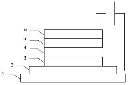
[0042] by figure 1 The structure shown is taken as an example, and the embodiment of the present invention also provides a method for preparing a quantum dot light-emitting diode, including the following steps:

[0043] provide the anode;

[0044] preparing a hole transport layer on the anode;

[0045] preparing a quantum dot luminescent layer on the hole transport layer;

[0046] An electron transport layer is prepared on the quantum dot luminescent layer; wherein, the preparation method of the electron transport layer specifically includes the steps of: preparing an inorganic layer on the quantum dot luminescent layer, preparing a metal layer on the inorganic layer, and preparing an organic layer on the metal layer;

[0047] A cathode is prepared on the electron transport layer.

[0048] In a preferred embodiment, in order to accelerate the alloying between the metal and the inorganic metal oxide, the prepared quantum dot light-emitting diode can be heat-treated. More p...

Embodiment 1

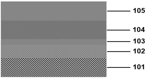
[0054] Example 1: Combining figure 2 As shown, the preparation method of the quantum dot light-emitting diode based on the inorganic / metal / organic composite structure electron transport layer comprises the following steps:

[0055]Using ITO as the anode, deposit 30nm-thick PEDOT:PSS as the hole injection layer on the surface of ITO under air environment, and anneal at 150°C for 10 minutes;

[0056] N 2 Under ambient conditions, a 30nm-thick TFB was deposited on the surface of the hole injection layer as a hole transport layer by solution method, and annealed at 150°C for 30 minutes;

[0057] N 2 Under ambient conditions, 25nm thick CdSe / ZnS quantum dots were deposited on the surface of the hole transport layer by solution method as the quantum dot light-emitting layer, and annealed at 100°C for 30 minutes;

[0058] N 2 Under ambient conditions, deposit 15nm thick ZnO as an inorganic layer on the surface of the quantum dot light-emitting layer by solution method, and annea...

Embodiment 2

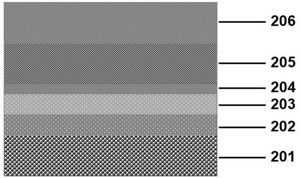
[0063] Example 2: Combining image 3 As shown, the preparation method of the quantum dot light-emitting diode based on the inorganic / inorganic metal / metal / organic composite structure electron transport layer comprises the following steps:

[0064] Using ITO as the anode, deposit 30nm-thick PEDOT:PSS as the hole injection layer on the surface of ITO under air environment, and anneal at 150°C for 10 minutes;

[0065] N 2 Under ambient conditions, a 30nm-thick TFB was deposited on the surface of the hole injection layer as a hole transport layer by solution method, and annealed at 150°C for 30 minutes;

[0066] N 2 Under ambient conditions, 25nm thick CdSe / ZnS quantum dots were deposited on the surface of the hole transport layer by solution method as the quantum dot light-emitting layer, and annealed at 100°C for 30 minutes;

[0067] Transfer the above substrate to the evaporation chamber, and vacuum to Below Pa, then evaporate and deposit 5nm thick ZnO as the inorganic lay...


PUM

PropertyMeasurementUnit
thicknessaaaaaaaaaa
thicknessaaaaaaaaaa
thicknessaaaaaaaaaa

Abstract

The invention discloses a quantum dot light-emitting diode, comprising: an anode, a cathode, a quantum dot light-emitting layer arranged between the anode and the cathode, and an electron transport layer arranged between the quantum dot light-emitting layer and the cathode, wherein, The electron transport layer includes: an inorganic layer, a metal layer and an organic layer, the inorganic layer is arranged close to the quantum dot light-emitting layer, the organic layer is arranged close to the cathode, and the metal layer is arranged between the inorganic layer and the Between the organic layers; the material of the inorganic layer includes a metal oxide, and the material of the organic layer includes an organic electron transport material. The invention provides an electron transport layer with an inorganic / metal / organic composite structure. On the basis of reducing the electron mobility of the electron transport layer and promoting the charge balance of quantum dot light-emitting diodes, it reduces the defect state of the inorganic / organic composite interface and reduces the interface impedance. , and reduce the oxygen vacancies of inorganic metal oxides, thereby improving the efficiency and lifetime of quantum dot light-emitting diodes.

Description

technical field [0001] The invention relates to the field of quantum dot light emitting devices, in particular to a quantum dot light emitting diode. Background technique [0002] Due to the unique optical properties of quantum dots, such as continuously adjustable emission wavelength with size and composition, narrow emission spectrum, high fluorescence efficiency, and good stability, quantum dot-based electroluminescent diodes have received extensive attention and research in the field of display. In addition, quantum dot light-emitting diode display also has many advantages that cannot be realized by LCD, such as large viewing angle, high contrast ratio, fast response speed, and flexibility, so it is expected to become the next generation of display technology. [0003] After decades of development, the performance of quantum dot light-emitting diodes has made great progress, one of the important reasons is the use of metal oxide nanoparticles as electron transport materi...

Claims


Application Information

Patent Timeline
Patent Type & Authority Patents(China)
IPC IPC(8): H01L51/50H01L51/54H01L51/56
CPCH10K85/649H10K85/30H10K50/115H10K50/166H10K2102/101H10K2102/00H10K71/00
Inventor 苏亮
Owner TCL CORPORATION
Why Eureka
Try Eureka