Interconnection structure, manufacturing method thereof and memory

A technology of interconnect structure and manufacturing method, which is applied in the field of semiconductors and can solve problems such as small critical dimensions and reduced reliability of semiconductor devices

Pending Publication Date: 2022-03-22
YANGTZE MEMORY TECH CO LTD
View PDF0 Cites 0 Cited by
  • Summary
  • Abstract
  • Description
  • Claims
  • Application Information

AI Technical Summary

Problems solved by technology

Among them, the critical dimensions of the interconnection structure used to realize the conduction of semi...

Method used


Image

  • Interconnection structure, manufacturing method thereof and memory
  • Interconnection structure, manufacturing method thereof and memory
  • Interconnection structure, manufacturing method thereof and memory

Examples


Embodiment Construction

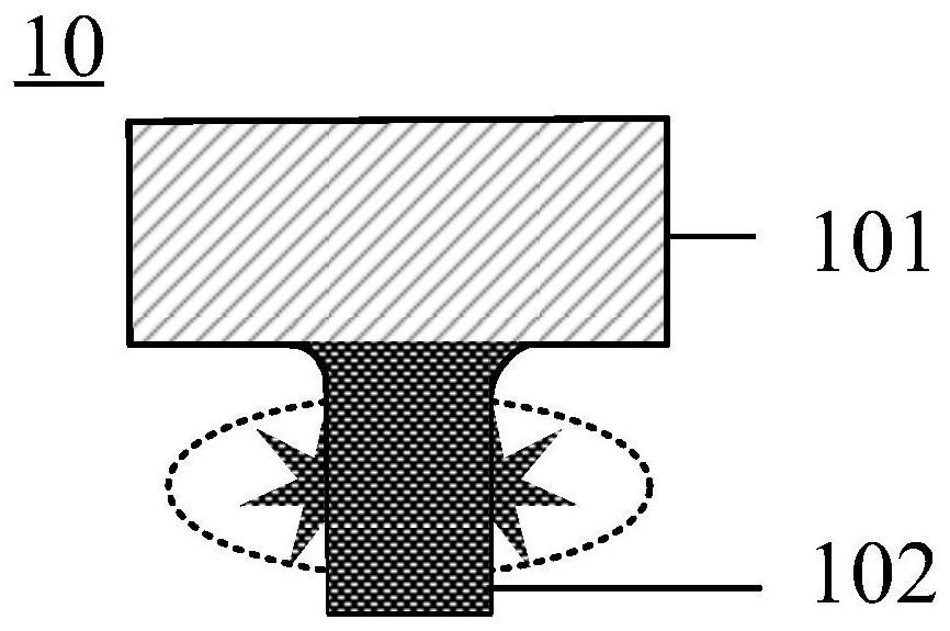
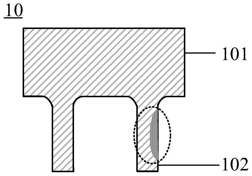
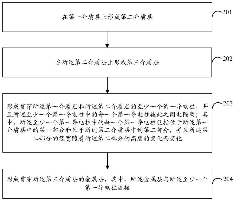
[0058] In order to make the technical solutions and advantages of the embodiments of the present invention clearer, the technical solutions of the present invention will be further described in detail below with reference to the drawings and embodiments. While the drawings show exemplary embodiments of the invention, it should be understood that the invention may be embodied in various forms and should not be limited to the embodiments set forth herein. Rather, these embodiments are provided for more thorough understanding of the present invention and to fully convey the scope of the present invention to those skilled in the art.

[0059] In the following paragraphs the invention is described more specifically by way of example with reference to the accompanying drawings. Advantages and features of the present invention will be apparent from the following description and claims. It should be noted that all the drawings are in a very simplified form and use imprecise scales, a...


PUM


Abstract

The invention provides an interconnection structure, a manufacturing method thereof and a memory. The interconnection structure comprises a first dielectric layer and a second dielectric layer, the second dielectric layer is located on the first dielectric layer; the third dielectric layer is located on the second dielectric layer; the at least one first conductive column penetrates through the first dielectric layer and the second dielectric layer, and all the first conductive columns in the at least one first conductive column are electrically isolated from one another, each first conductive column in the at least one first conductive column comprises a first part located in the first dielectric layer and a second part located in the second dielectric layer, and the diameter width of the second part is changed along with the change of the height of the second part; and the metal layer penetrates through the third dielectric layer, and the metal layer is connected with the at least one first conductive column.

Description

technical field [0001] The present invention relates to the technical field of semiconductors, and in particular, to an interconnection structure, a method for manufacturing the same, and a memory. Background technique [0002] With the rapid development of semiconductor technology, the application scope of semiconductor devices is rapidly expanding. Due to different requirements, the structural design of semiconductor devices is becoming more and more complex. In order to realize the miniaturization development of semiconductor devices, the structure size of semiconductor devices is getting smaller and smaller. Among them, the critical dimension of the interconnect structure for realizing the conduction of the semiconductor device is also becoming smaller and smaller, thereby reducing the reliability of the semiconductor device. SUMMARY OF THE INVENTION [0003] In order to solve the related technical problems, the embodiments of the present invention provide an interco...

Claims


Application Information

Patent Timeline
IPC IPC(8): H01L23/528H01L21/768
CPCH01L23/5283H01L21/76802H01L21/76816H01L21/76877H01L21/76882
Inventor 邹欣伟李威
Owner YANGTZE MEMORY TECH CO LTD
Why Eureka
Try Eureka