Field effect transistor using amorphous oxide film as channel layer, manufacturing method of field effect transistor using amorphous oxide film as channel layer, and manufacturing method of amorphous oxide film

a manufacturing method and technology of field effect transistor, applied in semiconductor/solid-state device manufacturing, semiconductor devices, electrical devices, etc., can solve the problems of inferior heat stability, inability to realize practical devices, and difficulty in forming tft on a substrate such as plastic plates or films, so as to reduce the hysteresis

Inactive Publication Date: 2010-09-07
CANON KK
View PDF22 Cites 583 Cited by
  • Summary
  • Abstract
  • Description
  • Claims
  • Application Information

AI Technical Summary

Benefits of technology

[0015]In addition, when an amorphous oxide material is used for a channel layer of a TFT, the electron carrier concentration is set in a desired range (such as in the range of approximately 1014 to 1018 / cm3). Furthermore, in order to ensure both reproducibility and uniformity of transistor properties, control means for accurately controlling the electron carrier concentration is provided.
[0016]In addition, by appropriately designing a method for forming an oxide material to be used for a channel of a transistor, the present invention also provides a method for forming a thin film having a desired electron carrier concentration with good control.

Problems solved by technology

However, in TFTs including an amorphous silicon TFT and a polycrystalline silicon TFT which have been developed heretofore, high temperature processes are required for device formation, and hence it has been difficult to form the TFT on a substrate such as a plastic plate or film.
However, the organic semiconductors such as pentacene disadvantageously have inferior heat stability (<150° C.) and toxicity (oncogenic properties), and hence practical devices have not been realized as of today.
However, since a compound primarily composed of ZnO cannot be formed into a stable amorphous phase at room temperature but is formed into a polycrystalline phase, the electron mobility cannot be increased due to scattering at interfaces of polycrystalline grains.
When the above TFT is used, for example, for a pixel circuit of a display device, the generation of the hysteresis as described above causes variation in operation of organic LED, liquid crystal, or the like which is to be driven, and as a result, the image quality of the display device is degraded.

Method used


Image

  • Field effect transistor using amorphous oxide film as channel layer, manufacturing method of field effect transistor using amorphous oxide film as channel layer, and manufacturing method of amorphous oxide film
  • Field effect transistor using amorphous oxide film as channel layer, manufacturing method of field effect transistor using amorphous oxide film as channel layer, and manufacturing method of amorphous oxide film
  • Field effect transistor using amorphous oxide film as channel layer, manufacturing method of field effect transistor using amorphous oxide film as channel layer, and manufacturing method of amorphous oxide film

Examples


example 1

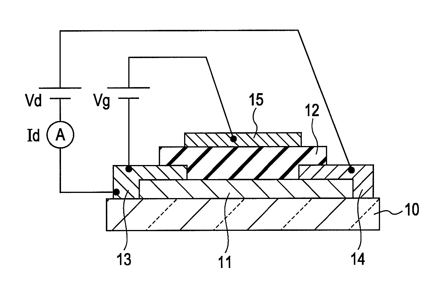
[0100]In this example, a top gate TFT shown in FIG. 1A was formed. In this example, the channel layer was an In—Ga—Zn—O-based amorphous oxide formed by a sputtering method in a hydrogen-containing atmosphere.

[0101]First, on a glass substrate (Corning #1737 glass manufactured by Corning Incorporated), an amorphous oxide film containing hydrogen was formed as the channel layer.

[0102]In this example, an In—Ga—Zn—O-based amorphous oxide film containing hydrogen was formed by high-frequency sputtering in a mixed gas atmosphere containing an argon, an oxygen, and a hydrogen gas.

[0103]A sputtering apparatus as shown in FIG. 5 was used. In this figure, reference numeral 51 indicates a sample, reference numeral 52 a target, reference numeral 53 a vacuum pump, reference numeral 54 a vacuum gauge, reference numeral 55 a substrate holder, reference numeral 56 gas flow-rate controller provided for each gas introduction system, reference numeral 57 a pressure controller, and reference numeral 58 ...

example 2

[0128]In this example, an amorphous oxide film containing hydrogen will be described which is to be used for a channel layer of a thin-film transistor. First, an insulating thin film of an amorphous oxide was formed on a quartz substrate.

[0129]A film-forming method of the amorphous oxide was performed in accordance with that described in Example 1. The target (material source) was InGaO3(ZnO), and the total pressure in an atmosphere during film formation was 0.3 Pa. In this step, the gas flow rate ratio was set to Ar:O2=95:5, and hence the oxygen partial pressure corresponded to 0.015 Pa. In addition, a hydrogen gas was not supplied. The film thickness was set to approximately 400 nm. When the resistance of the thin film thus formed was measured by a four probe method, the conductivity was not more than the measurement limit (0.0001 S / cm or less), and hence it was confirmed that the thin film was an insulating film.

[0130]Next, hydrogen ion implantation was performed for the above am...

example 3

[0137]In this example, a top gate TFT shown in FIG. 1A was formed. In this case, a channel layer of an amorphous oxide containing hydrogen (or deuterium) was formed by ion implantation of hydrogen or deuterium in an In—Ga—Zn—O-based amorphous oxide formed by a pulse laser deposition method (PLD method).

[0138]First, on a glass substrate (Corning #1737 glass manufactured by Corning Incorporated), an In—Zn—Ga—O-based amorphous oxide film was formed by the PLD method.

[0139]A polycrystalline sintered material of InGaO3(ZnO)4 was used as the target, and an In—Zn—Ga—O-based amorphous oxide film was deposited. The oxygen partial pressure was 7 Pa during the film formation. The power of a KrF excimer laser was 1.5×10⁻³ mJ / cm2 / pulse, the pulse width was 20 nsec, and the repeated frequency was 10 Hz. In addition, the substrate temperature was unheated and kept around room temperature of 25° C.

[0140]According to the results of a fluorescent x-ray (XRF) analysis, as the metal composition ratio o...


PUM

PropertyMeasurementUnit
gate voltage Vgaaaaaaaaaa
voltageaaaaaaaaaa

Abstract

An amorphous oxide containing hydrogen (or deuterium) is applied to a channel layer of a transistor. Accordingly, a thin film transistor having superior TFT properties can be realized, the superior TFT properties including a small hysteresis, normally OFF operation, a high ON / OFF ratio, a high saturated current, and the like. Furthermore, as a method for manufacturing a channel layer made of an amorphous oxide, film formation is performed in an atmosphere containing a hydrogen gas and an oxygen gas, so that the carrier concentration of the amorphous oxide can be controlled.

Description

TECHNICAL FIELD[0001]The present invention relates to a field effect transistor which has a channel layer formed from an amorphous oxide and which has transistor properties applicable to a display device and the like.BACKGROUND ART[0002]A field effect transistor (hereinafter referred to as “FET” in some cases) has a gate electrode, a source electrode, and a drain electrode. In addition, the field effect transistor is an active device in which current flowing in the channel layer, that is, current flowing between the source and the drain electrodes is controlled by applying a voltage to the gate electrode. In particular, an FET using a thin film formed on an insulating substrate of a ceramic, a glass, or a plastic as a channel layer is called a thin film transistor (hereinafter referred to as “TFT” in some cases).[0003]The TFT can be advantageously easily formed on a relatively large substrate by using techniques to form thin films, and as a result, the TFT has been widely used as a ...

Claims


Application Information

Patent Timeline
Patent Type & Authority Patents(United States)
IPC IPC(8): H01L29/04H01L29/15
CPCH01L29/78693H01L29/66969Y10T29/41H01L29/06H01L29/66742
Inventor IWASAKI, TATSUYA
Owner CANON KK
Why Eureka
Try Eureka