Method for Forming SiOCH Film Using Organoaminosilane Annealing

a technology of organoaminosilane and film, which is applied in the direction of semiconductor/solid-state device manufacturing, basic electric elements, electric apparatus, etc., can solve the problems of large film shrinkage, increased wiring capacitance, and signal delay due to the resultant, so as to reduce the amount of components, increase the quantity of components, and high flowability

Active Publication Date: 2015-02-26
ASM IP HLDG BV
View PDF1 Cites 254 Cited by
  • Summary
  • Abstract
  • Description
  • Claims
  • Application Information

AI Technical Summary

Benefits of technology

[0007]In some embodiments, after depositing a low-k film (such as SiOCH film) having high flowability, the film is subjected to a step of exposing the film to a reactive gas (such as organoaminosilane) which is reactive to —OH groups. Since highly flowable SiOCH film contains many unstable groups (such as alcohol groups, hydroxyl groups), by introducing the above gas, the unstable grou

Problems solved by technology

With miniaturization of wiring pitch of large scale integration (LSI) devices, signal delay due to the resultant increased wiring capacitance has become a problem.
Due to the occurrence of desorption or cross-linkage of these components during curing, extensive film shrinkage occurs.
As a result, because voids are generated in the film which is

Method used


Image

  • Method for Forming SiOCH Film Using Organoaminosilane Annealing
  • Method for Forming SiOCH Film Using Organoaminosilane Annealing
  • Method for Forming SiOCH Film Using Organoaminosilane Annealing

Examples


example 1

[0129]In this example, a carbon-doped silicon oxide film was formed on a substrate as follows:

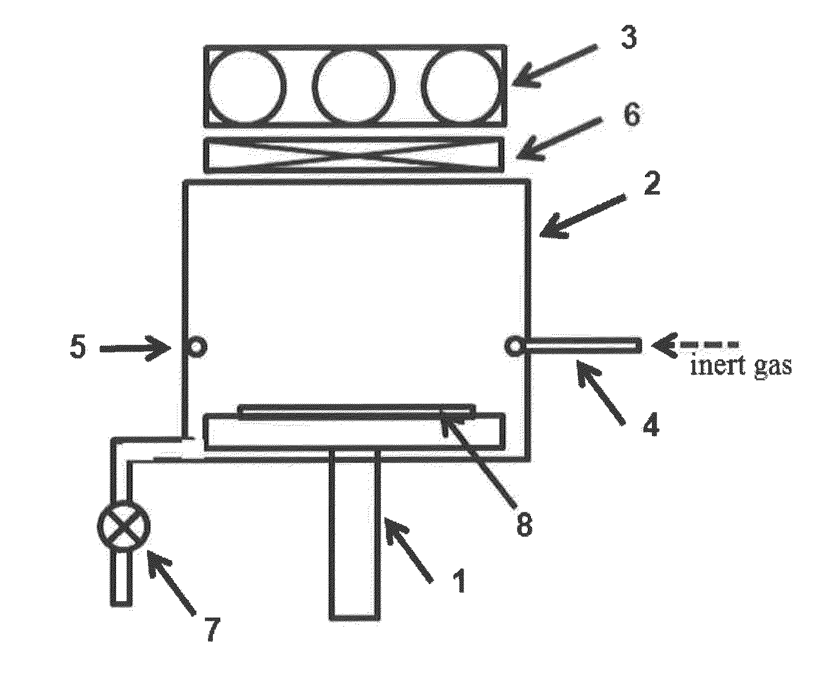
[0130](1) placing a patterned substrate on a lower electrode whose temperature was controlled at about 20° C. in a vacuum environment in a plasma reactor;

[0131](2) supplying about 0.3 g / min of siloxane (diethoxymethylsilane), about 40 sccm of oxidizing gas (oxygen), and about 300 sccm of rare gas (He) to the reactor and controlling the pressure in the reactor at about 300 Pa;

[0132](3) generating a plasma by applying RF power (about 13 MHz, about 100 W) to the reactor;

[0133](4) forming a gap-fill low-k film on the patterned substrate due to reaction of the gases using the plasma;

[0134](5) after evacuating the reactor, supplying about 100 sccm of a gas containing about 30% of dimethylaminotrimethylsilane in rare gas (Ar) and controlling the pressure in the reactor at about 1,200 Pa, thereby exposing the film to the dimethylaminotrimethylsilane gas for 2 minutes at a temperature of about 25° C...

example 2

[0142]Multiple substrates were continuously processed under conditions which were substantially similar to those in Example 1, using the clustered apparatus illustrated in FIG. 4, wherein each substrate was transferred between the chambers via the transfer chamber 41 so that the substrate was not exposed to the outside atmosphere. While transferring the substrates between the chambers, the pressure of the transfer chamber was adjusted at a pressure (100 to 1,500 mTorr) higher than that in the film formation chamber using nitrogen gas. As a comparative example, multiple substrates were processed under the same conditions except that the substrates were processed by batch at each chamber (25 wafers constituted one batch or lot), wherein the transfer chamber was not used so that the substrates were exposed to the outside atmosphere until all the substrates of the lot were processed.

[0143]FIG. 5 is a graph showing the relationship between thickness (a.u.) of cured film and cumulative nu...

example 3

[0145]In this example, a carbon-doped silicon oxide film was formed on a substrate as follows:

[0146](1) placing a patterned substrate on a lower electrode whose temperature was controlled at about 20° C. in a vacuum environment in a plasma reactor;

[0147](2) supplying about 0.3 g / min of siloxane (diethoxymethylsilane), about 40 sccm of oxidizing gas (oxygen), and about 300 sccm of rare gas (He) to the reactor and controlling the pressure in the reactor at about 300 Pa;

[0148](3) generating a plasma by applying RF power (about 13 MHz, about 100 W) to the reactor;

[0149](4) forming a gap-fill low-k film on the patterned substrate due to reaction of the gases using the plasma;

[0150](5) starting supplying about 1,000 sccm of oxygen (O2) and about 5,000 sccm of rare gas (Ar) to a remote plasma unit upstream of the reactor so as to supply an oxygen plasma to the reactor while controlling the pressure in the reactor at about 1,000 Pa;

[0151](6) after evacuating the reactor, supplying about 100...


PUM


Abstract

A method for forming a modified low-k SiOCH film on a substrate, includes: providing a low-k SiOCH film formed on a substrate by flowable CVD; exposing the low-k SiOCH film to a gas containing a Si—N bond in its molecule without applying electromagnetic energy to increase Si—O bonds and/or Si—C bonds in the film; and then curing the low-k SiOCH film.

Description

FIELD OF THE INVENTION[0001]The present invention generally relates to a method for forming a carbon-doped silicon oxide (SiOCH) film on a substrate, particularly to a method for forming a SiOCH film modified by organoaminosilane annealing, for example.DESCRIPTION OF THE RELATED ART[0002]With miniaturization of wiring pitch of large scale integration (LSI) devices, signal delay due to the resultant increased wiring capacitance has become a problem. In order to reduce the wiring capacitance, attempts to reduce the dielectric constant of interlayer films have been implemented, and as a result, porous SiOCH films having pores in the films have been utilized.[0003]Recently, instead of the damascene process used for conventional Cu wiring, a process of forming metal wires and embedding low-K film (e.g., a SiOCH film) between them is considered. For the process, a method of forming highly flowable film at a low temperature is required.[0004]In forming flowable low-k film, it is necessary ...

Claims


Application Information

Patent Timeline
IPC IPC(8): H01L21/02
CPCH01L21/02126H01L21/02348H01L21/02211H01L21/02271H01L21/02216H01L21/02274H01L21/02323H01L21/02337H01L21/0234H01L21/67115H01L21/67207H01L21/324
Inventor ISHIKAWA, DAIMATSUSHITA, KIYOHIRONAKANO, AKINORIUEDA, SHINTAROARAI, HIROFUMI
Owner ASM IP HLDG BV
Why Eureka
Try Eureka