

High performance strained silicon FinFETs device and method for forming same
a technology of fin field effect transistor and high-performance strained silicon, which is applied in the direction of semiconductor devices, electrical devices, transistors, etc., can solve the problems of difficult integration of strained silicon, difficult to control the thickness of the channel, and strained silicon channels that have not been demonstrated in devices as small as 50 nm, so as to improve device performance and yield. , the effect of improving the mobility of the channel
- Summary
- Abstract
- Description
- Claims
- Application Information
AI Technical Summary
Benefits of technology
Problems solved by technology
Method used
Image

Examples
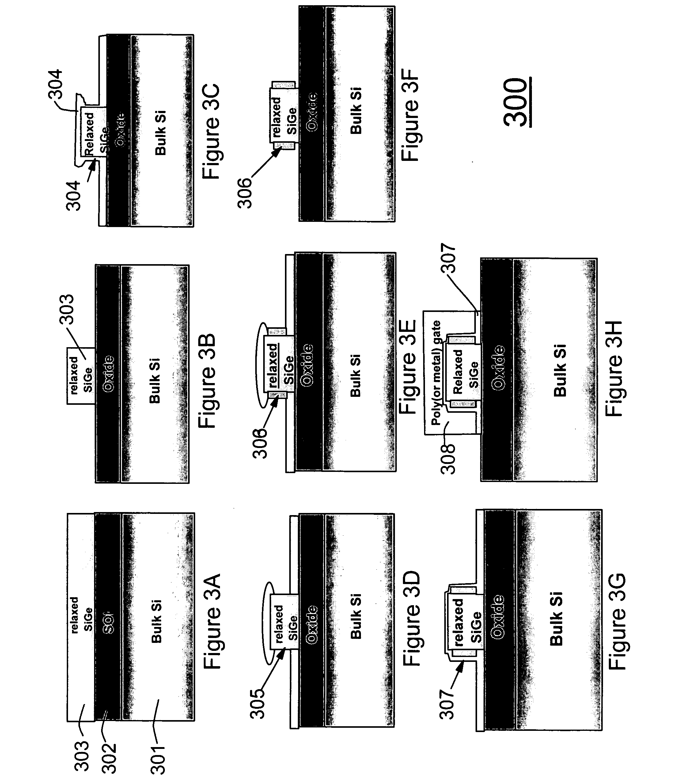
second exemplary embodiment
[0073] A second exemplary embodiment, as shown in FIGS. 4A-4E, is advantageous as it allows the invention to minimize the number of mask steps. Indeed, it allows the invention to avoid a mask step since as shown and described below, there is a fin oxide hard mask above, and an oxide layer below, the relaxed SiGe layer. It is noted that thin silicon (˜5-10 nm) from the SOI is removed after the SiGe Fin RIE.
[0074] As a result, the second exemplary embodiment provides a process which is automatically self-aligned, thereby providing a more simple and elegant method even for a small gate. Hence, this embodiment provides self-aligned masking for selective growth. Moreover, there is no need to remove the hard mask to dope the top of the structure, as the invention allows doping on the sides of the structure.
[0075] Turning now to FIGS. 4A-4E and the flowchart 450 of FIG. 4F, a process of forming a FinFET 400 according to the present invention is shown.
[0076] First, in FIG. 4A (and step 4...
PUM
 Abstract
Description
Claims
Application Information