

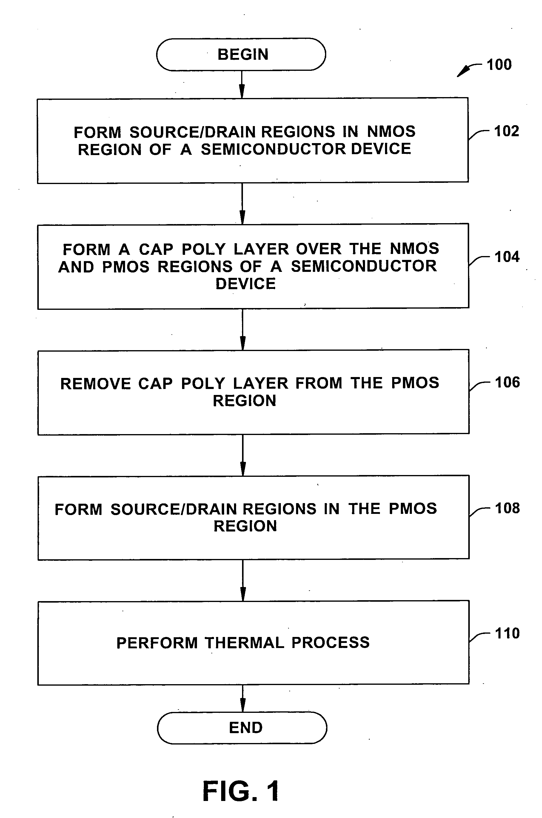
Method to selectively strain NMOS devices using a cap poly layer
a technology of nmos devices and polylayers, applied in the field of transistors, can solve the problems of degrading the performance of pmos devices and hole mobility, and achieve the effects of preventing or mitigating tensile stress, improving channel mobility of nmos devices, and facilitating semiconductor fabrication
- Summary
- Abstract
- Description
- Claims
- Application Information
AI Technical Summary
Benefits of technology
Problems solved by technology
Method used
Image

Examples
Embodiment Construction
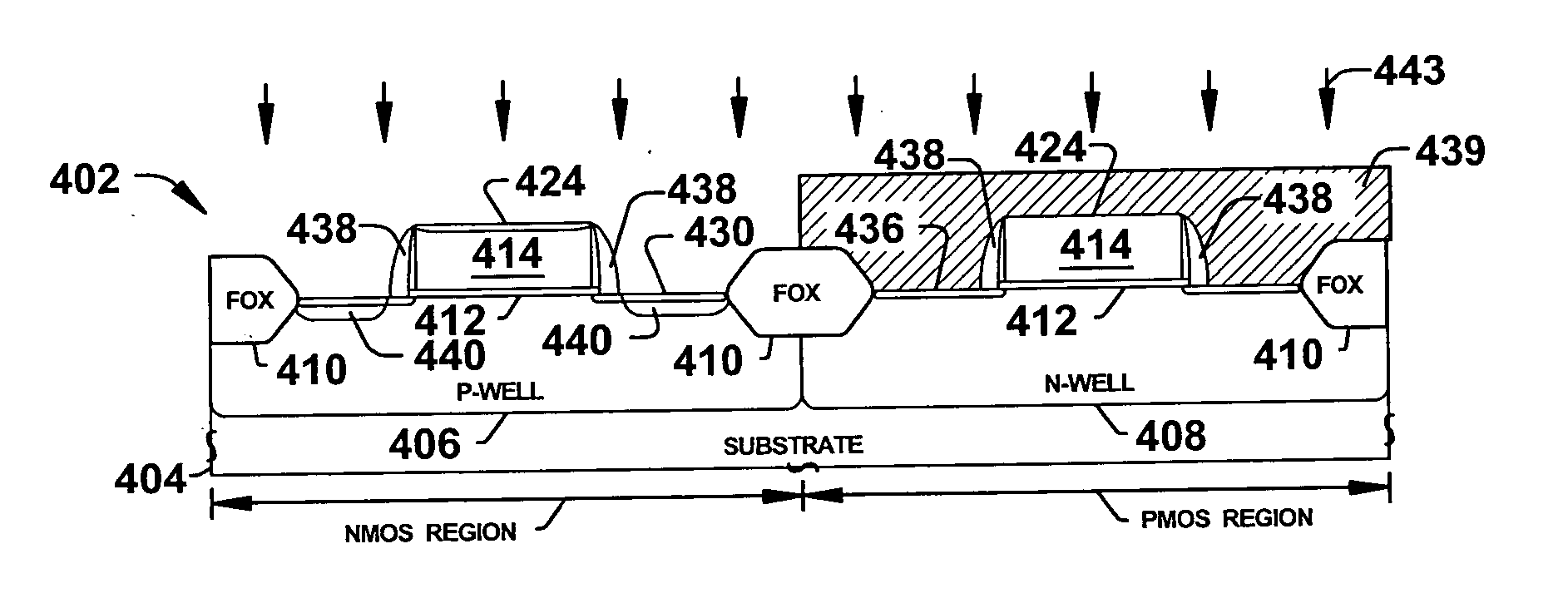
[0014] One or more implementations of the present invention will now be described with reference to the attached drawings, wherein like reference numerals are used to refer to like elements throughout, and wherein the illustrated structures are not necessarily drawn to scale. The invention provides transistor structures and methods in which transistor mobility is improved while reducing masks employed in fabrication thereof.
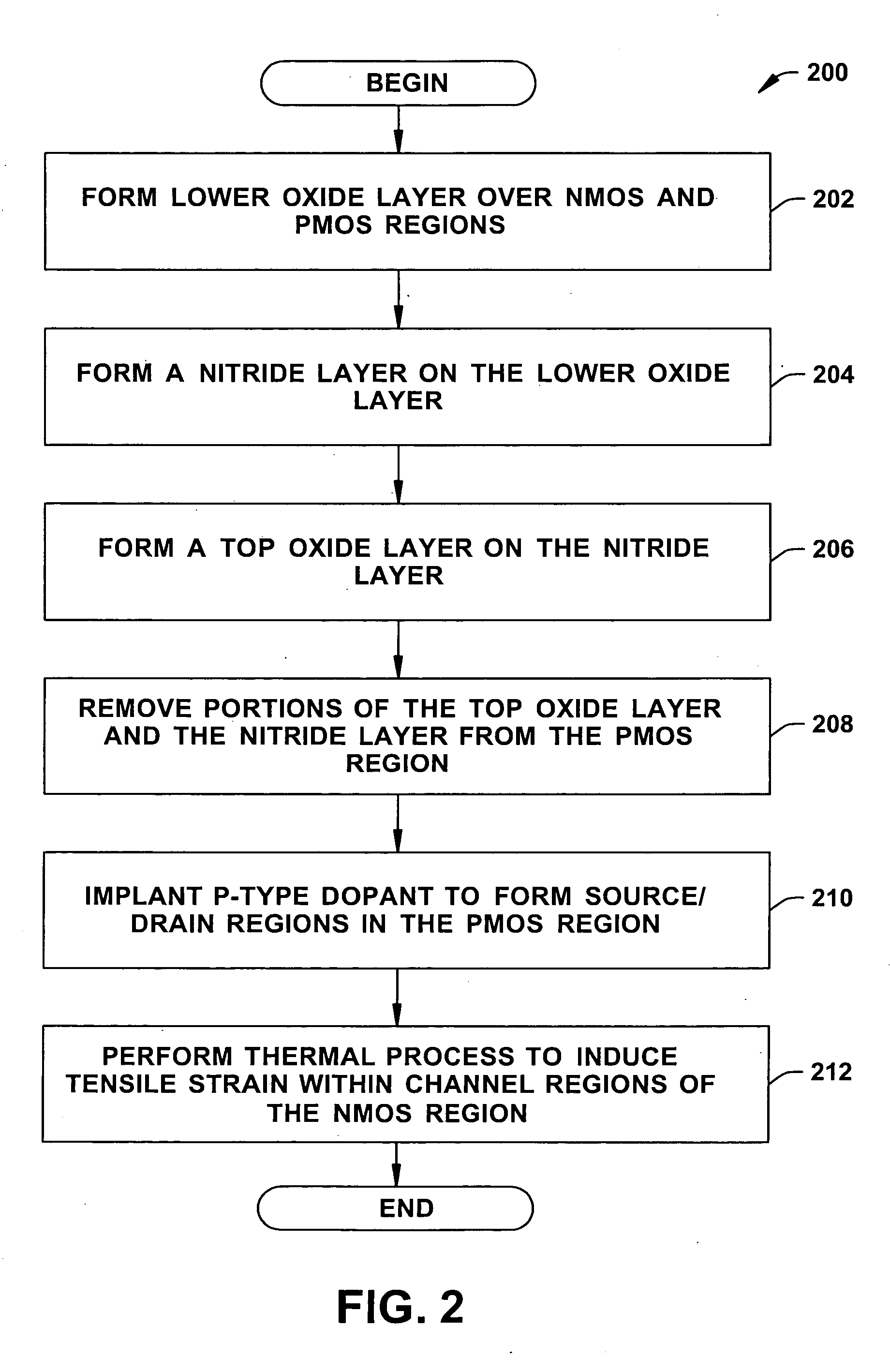
[0015] The present invention facilitates semiconductor fabrication by providing methods of fabrication that selectively apply tensile strain to channel regions of devices while mitigating masking operations employed. A cap poly layer is formed over NMOS and PMOS regions of a semiconductor device. Then, a resist mask is employed to remove a portion of the cap poly layer from the PMOS region. Subsequently, the same resist mask and / or remaining portion of the cap poly layer is employed to form source / drain regions within the PMOS region by implanting a p-type dopan...
PUM
 Abstract
Description
Claims
Application Information