Maskless multiple sheet polysilicon resistor

a polysilicon resistor, maskless technology, applied in the direction of semiconductor devices, diodes, electrical devices, etc., to achieve the effect of facilitating semiconductor fabrication

Active Publication Date: 2006-10-19
TEXAS INSTR INC
View PDF16 Cites 16 Cited by
  • Summary
  • Abstract
  • Description
  • Claims
  • Application Information

AI Technical Summary

Benefits of technology

[0008] The present invention facilitates semiconductor fabrication by forming polysilicon resistors having varied sheet resistance values in a single mask, single doping operation. The present invention employs masks that selectively expose portions of polysilicon resistor structures thereby controlling dopant concentration, instead of employing discrete ion doping processes to achieve varied concentrations.

Problems solved by technology

Unfortunately, obtaining these varied dopant types and / or amounts requires discrete doping processes, including ion implantation and diffusion, which typically require separate masks and patterning operations.

Method used


Image

  • Maskless multiple sheet polysilicon resistor
  • Maskless multiple sheet polysilicon resistor
  • Maskless multiple sheet polysilicon resistor

Examples


Embodiment Construction

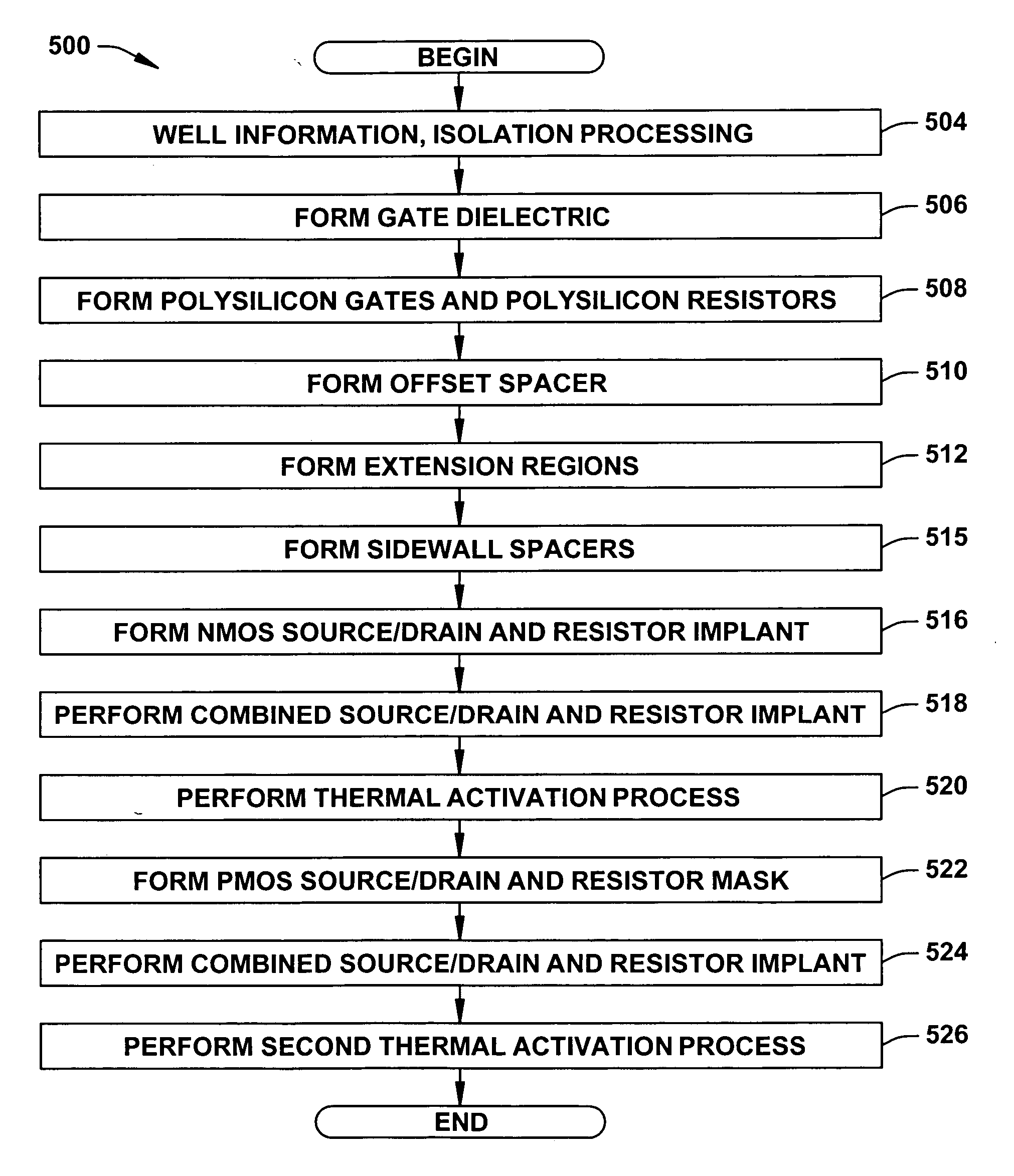
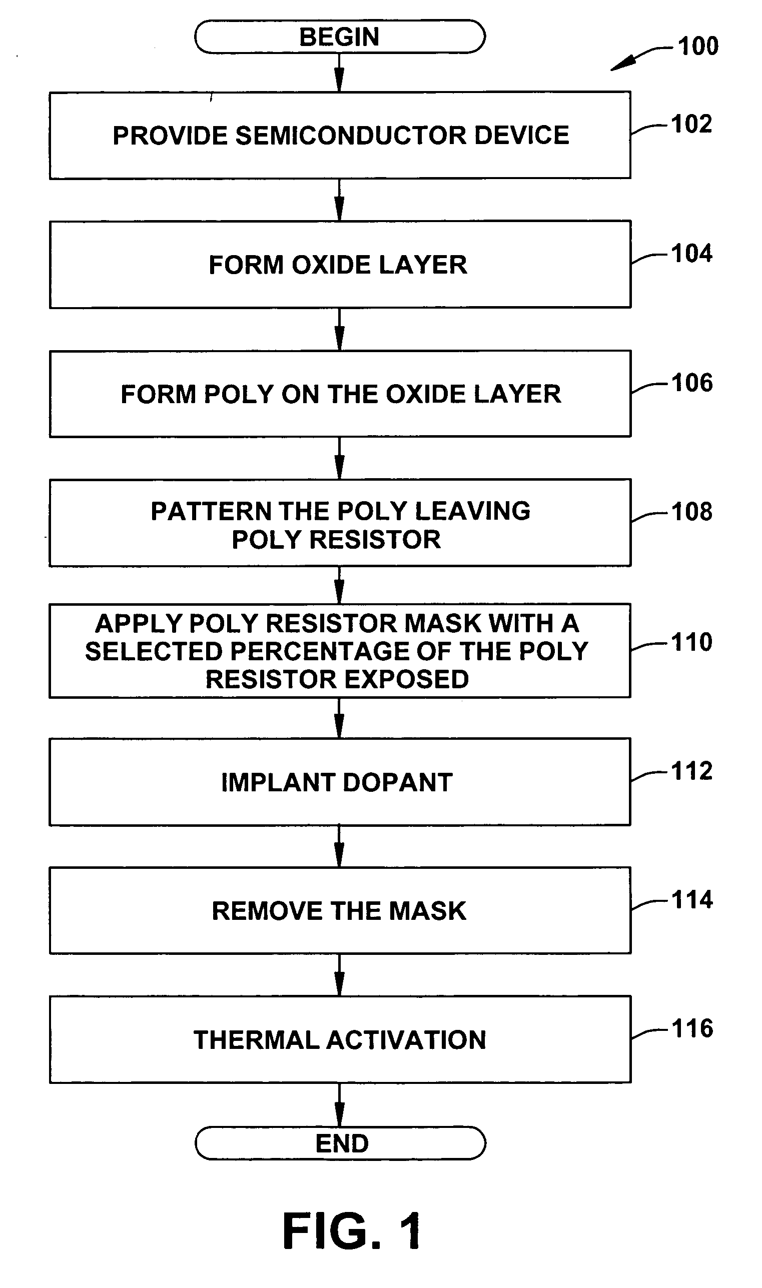
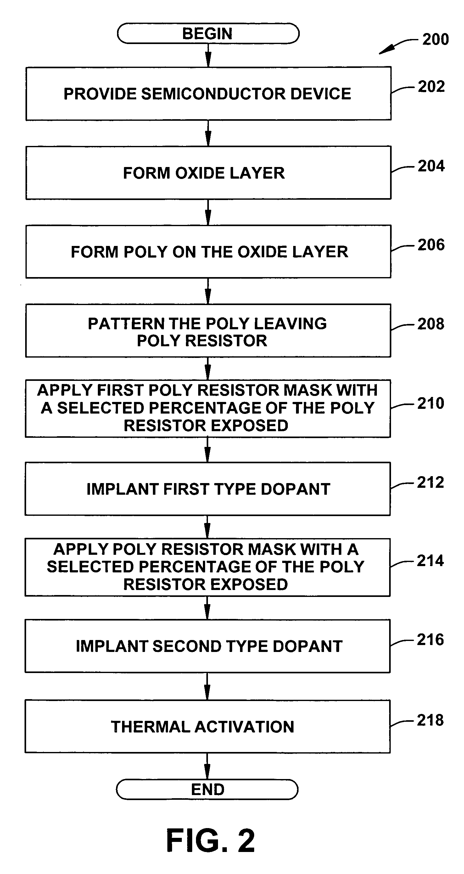
[0019] One or more implementations of the present invention will now be described with reference to the attached drawings, wherein like reference numerals are used to refer to like elements throughout, and wherein the illustrated structures are not necessarily drawn to scale.

[0020] Forming polysilicon resistors on the same wafer / device as other circuit components can be difficult. One reason is that the thickness of the polysilicon layer is generally determined by the required characteristics of other devices. For example, the deposited polysilicon is also employed to form the gates and / or emitters of active components and capacitor plates. This can require thicknesses greater than, for example 200 nanometers.

[0021] Polysilicon resistivity is a non-linear function of doping wherein the resistivity decreases as the doping dose increases. This resistivity, also referred to as sheet resistance, is expressed in ohms-cm and has an upper limit based on implant dose control (e.g., 0.060 ...


PUM


Abstract

The present invention facilitates semiconductor fabrication of semiconductor devices having polysilicon resistors. An oxide layer is formed over a semiconductor device (104). A polysilicon layer is formed on the oxide layer (106). The polysilicon layer is patterned to form a polysilicon resistor (108). A poly resistor mask having a selected percentage of the poly resistor exposed is formed on the poly resistor (110). A selected dopant is implanted (112), which modifies the resistivity of the poly resistor. The mask is removed (114) and a thermal activation process is performed (116) that diffuses the implanted dopant to a substantially uniform concentration throughout the polysilicon resistor.

Description

FIELD OF INVENTION [0001] The present invention relates generally to semiconductor devices and more particularly to polysilicon resistors and fabrication thereof. BACKGROUND OF THE INVENTION [0002] Semiconductor device fabrication involves performing a variety of processes, procedures and operations in order to achieve a fabricated device. These operations include, but are not limited to, layering, doping, heat treatments, and patterning. Layering is the operation used to add layers of a selected thickness to a wafer surface. These layers can be insulators, semiconductors, conductors, and the like and can be grown or deposited by a number of suitable methods (e.g., chemical vapor deposition, sputtering, and the like). [0003] Doping is the process that introduces specific amounts of dopants in the wafer surface through openings in surface layers. Two general techniques of doping are thermal diffusion and ion implantation. Doping is used, for example, to create active regions in trans...

Claims


Application Information

Patent Timeline
Patent Type & Authority Applications(United States)
IPC IPC(8): H01L21/8244H01L21/8222H01L21/8234
CPCH01L27/0203H01L28/20H01L27/0802H01L27/0629
Inventor HOWARD, GREGORY ERICSWANSON, LELAND
Owner TEXAS INSTR INC
Why Eureka
Try Eureka