Semiconductor light emitting element, group iii nitride semiconductor substrate and method for manufacturing such group iii nitride semiconductor substrate

a technology of nitride and semiconductor substrates, which is applied in the direction of crystal growth process, monocrystalline material growth, semiconductor lasers, etc., can solve the problems of insufficient crystallinity of gan thin film obtained through heteroepitaxial growth by vapor-phase epitaxial growth, insufficient dislocation density, and insufficient production process. achieve excellent light extraction properties, control of dopant concentration, and control of transparency

Inactive Publication Date: 2010-09-16
PANASONIC CORP
View PDF13 Cites 28 Cited by
  • Summary
  • Abstract
  • Description
  • Claims
  • Application Information

AI Technical Summary

Benefits of technology

[0015]According to the present invention, a semiconductor light-emitting element can be obtained that has an excellent light extraction property. Moreover, according to the present invention, a group III semiconductor substrate can be obtained having a controlled dopant concentration and controlled transparency.

Problems solved by technology

Therefore, the crystallinity of a GaN thin film obtained through heteroepitaxial growth by vapor-phase epitaxial growth is not sufficient.
Although by using this method, dislocation density can be reduced to about 106 to about 107 cm−2, the production process is troublesome.
However, these methods cannot sufficiently reduce dislocation density and result in a structure in which dislocation is locally concentrated.
Therefore, it is difficult to produce LDs and LEDs of high intensity and high reliability with such substrates.
However, it is known that when Ge is used for doping in a high concentration (for example, 1×1019 cm3) by vapor phase epitaxy, pit-like defects are generated on a crystalline thin film and enhancing the mobility is troublesome (Non-Patent Documents 1 and 2).
In addition, in an LD using a group III nitride substrate, due to light escaping from the active layer into the group III nitride substrate side and due to the fact that light escaping onto the p-side electrode is reflected on the group III nitride substrate and as a result escapes to the group III nitride substrate side, there is a problem that a disruption is observed in the emission pattern (interference pattern and substrate propagation mode) of the LD (Patent Document 5).

Method used


Image

  • Semiconductor light emitting element, group iii nitride semiconductor substrate and method for manufacturing such group iii nitride semiconductor substrate
  • Semiconductor light emitting element, group iii nitride semiconductor substrate and method for manufacturing such group iii nitride semiconductor substrate
  • Semiconductor light emitting element, group iii nitride semiconductor substrate and method for manufacturing such group iii nitride semiconductor substrate

Examples


embodiment 1

[0097]A method for producing a group III nitride semiconductor substrate according to the present invention is described below.

[0098]First, the desired amounts of a group III element, alkali metal element and / or alkaline earth metal element, and germanium are weighed out in an inert atmosphere such as in a glove box or the like and then introduced into a crucible. A seed crystal simultaneously is placed in the crucible as necessary. Any crystal can be used as the seed crystal. Usually, a seed crystal of a substrate in which a GaN crystal has been grown by vapor phase epitaxy on a sapphire or SiC crystal to the thickness of, for example, about 1 to about 20 μm can be used advantageously to produce a group III nitride semiconductor substrate having a greater area. Moreover, it is possible to use as a seed crystal, for example, a crystal having a diameter of 20 mm to 5 inches obtained by liquid phase or vapor phase epitaxy.

[0099]Next, the crucible is fixed to a reactor or pressure vess...

example 1

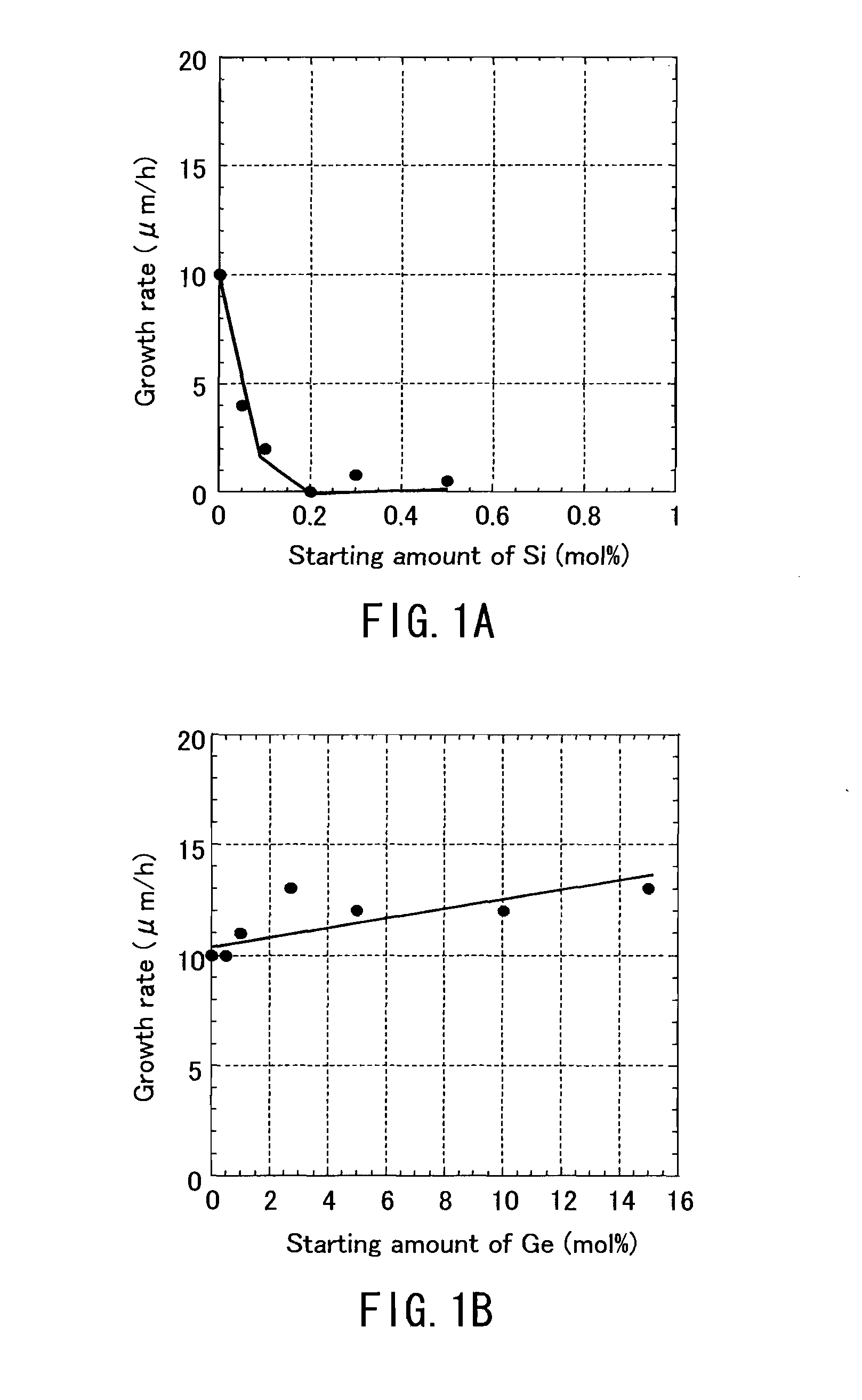
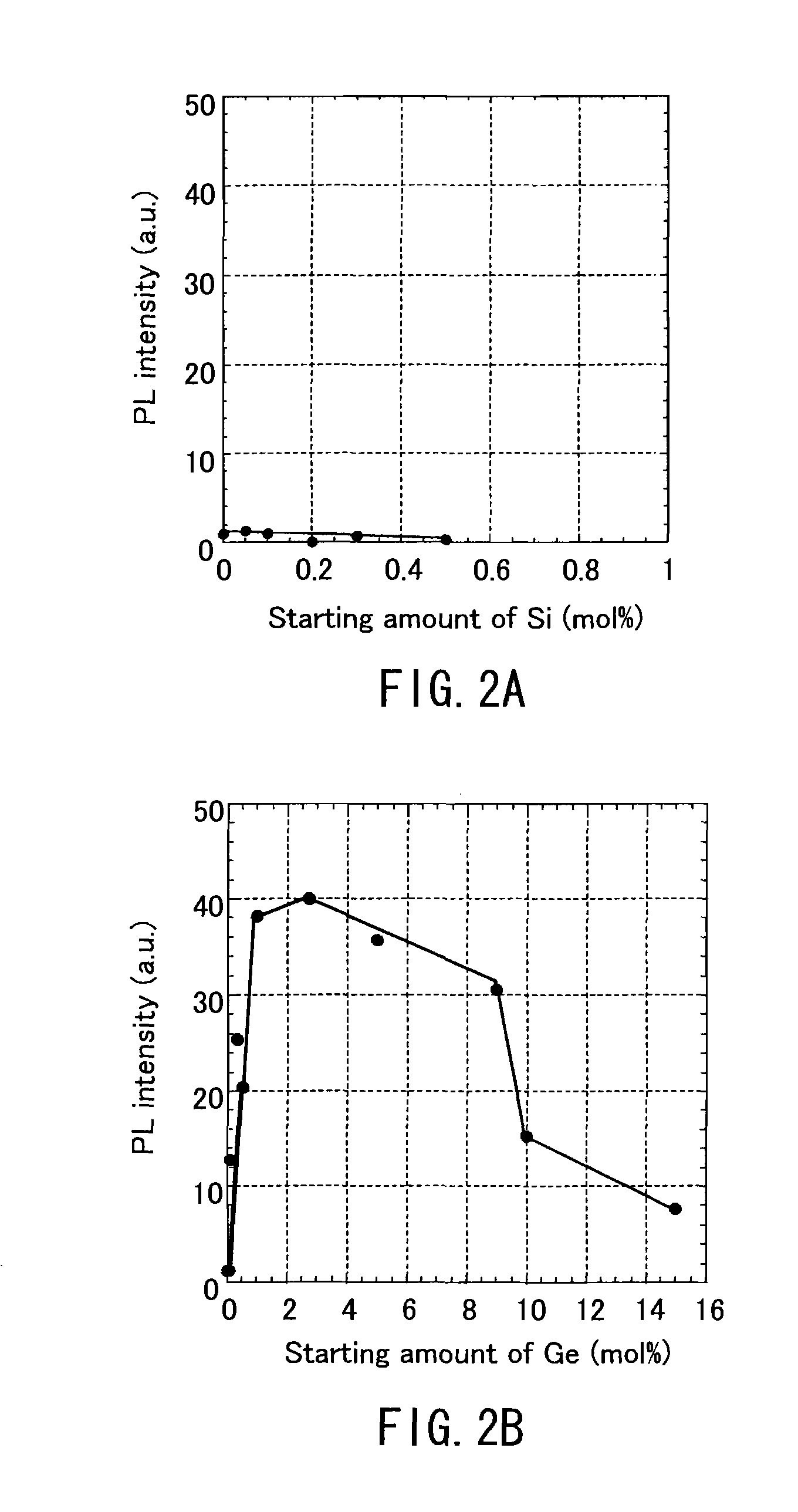
[0114]In this example, Na was used as an alkali metal, Ga was used as a group III element, nitrogen gas was used as a nitrogen source, Ge was used as a dopant, and 10 mm per to side 1-inch GaN crystals were grown by LPE with various starting amounts of Ge in melts.

[0115]Used as a seed substrate was a substrate having a GaN layer with a thickness of 5 to 10 μm which had been grown by vapor phase epitaxy on a support substrate (sapphire). A GaN crystal containing Ge as a dopant was grown by vapor phase epitaxy on the seed substrate under conditions of a crystal growth temperature of 850 to 880° C. and a growth pressure of 2.5 to 4 MPa. The surface of the obtained crystal was subjected to machine polishing, mechanical chemical polishing, dry etching, etc., thereby obtaining a sapphire substrate-containing GaN substrate having a square 10 mm per side to a diameter of 1 inch. Moreover, when necessary, the sapphire substrate and the like were removed using methods such as laser lift-off, ...

example 2

[0123]Another example of a method for producing a GaN substrate according to the present invention is described below using FIG. 5. Described is a case where a GaN substrate is grown using a Na flux, but basically the same method is applicable to other group III nitride crystals as well.

[0124]First, a flux, i.e., Na, and the starting materials, i.e., Ga and the desired proportion of Ge, and a seed substrate were introduced into a crucible. A substrate on which a GaN thin film 12 (thickness: 10 μm) had been grown from vapor phase on a sapphire substrate 11 having a diameter of 1 inch was used as a seed substrate. Here, in order to avoid, for example, the oxidation of Na, introduction of the starting materials and the seed substrate into the crucible and reactor is carried out in a glove box replaced with an inert gas such as nitrogen gas, Ar gas or the like. After placing the reactor in a crystal growth furnace, the reactor may be evacuated and then pressurized with nitrogen as neces...


PUM

PropertyMeasurementUnit
optical absorption coefficientaaaaaaaaaa
diameteraaaaaaaaaa

Abstract

An object of the present invention is to obtain, with respect to a semiconductor light-emitting element using a group III nitride semiconductor substrate, a semiconductor light-emitting element having an excellent light extraction property by selecting a specific substrate dopant and controlling the concentration thereof. The semiconductor light-emitting element comprises a substrate composed of a group III nitride semiconductor comprising germanium (Ge) as a dopant, an n-type semiconductor layer composed of a group III nitride semiconductor formed on the substrate, an active layer composed of a group III nitride semiconductor formed on the n-type semiconductor layer, and a p-type semiconductor layer composed of a group III nitride semiconductor formed on the active layer in which the substrate has a germanium (Ge) concentration of 2×10¹⁷ to 2×1019 cm−3. The substrate is produced in a nitrogen-containing atmosphere using a melt comprising at least a group III element, an alkali or alkaline earth metal, and germanium (Ge) and nitrogen.

Description

TECHNICAL FIELD[0001]The present invention relates to a semiconductor light-emitting element such as a blue light-emitting diode (blue LED), blue laser diode (blue LD) or the like formed on a group III nitride semiconductor substrate, a group III nitride semiconductor substrate for use therefor, and a method for manufacturing such group III nitride semiconductor substrate.BACKGROUND ART[0002]Gallium nitride (GaN), aluminum nitride (AlN), AlGaN, InGaN, AlGaInN and other group III nitride semiconductors have been attracting attention as materials for semiconductor light-emitting element that emit blue light or ultraviolet light. Blue laser diodes (blue LDs) are applied to high-density optical disks and displays, and blue light-emitting diodes (blue LEDs) are applied to displays, illuminations and the like. Furthermore, ultraviolet LDs are expected to be useful for biotechnology, and ultraviolet LEDs are expected to be a source of ultraviolet light in fluorescent lamps.[0003]Group III ...

Claims


Application Information

Patent Timeline
Patent Type & Authority Applications(United States)
IPC IPC(8): H01L33/30C30B19/02H01L33/62H01L33/32
CPCC30B19/02C30B29/403C30B29/406H01L33/025H01L33/0075H01S5/0206H01S5/22H01S5/305H01S5/32341H01L33/32
Inventor MINEMOTO, HISASHIKITAOKA, YASUOKAWAGUCHI, YASUTOSHITAKAHASHI, YASUHITOHASEGAWA, YOSHIAKI
Owner PANASONIC CORP
Why Eureka
Try Eureka