Method to strain NMOS devices while mitigating dopant diffusion for PMOS using a capped poly layer

Active Publication Date: 2006-08-24
TEXAS INSTR INC
View PDF7 Cites 3 Cited by
  • Summary
  • Abstract
  • Description
  • Claims
  • Application Information

AI Technical Summary

Benefits of technology

[0008] The present invention facilitates semiconductor fabrication by applying tensile stress to channel regions of NMOS devices while mitigating degradation to PMOS devices due to undesired p-type dopant diffusion. The present invention forms source/drain regions in the PMOS region and then performs a thermal process that mitigates p-type dopant diffusion during formation of a capped poly layer and subsequent strain inducing thermal process.
[0009] The present invention forms and activates source/drain regions within a PMOS region prior to forming a capped poly layer. A thermal process is performed after forming the source/drain regions that activates the dopants. Subsequently, source/drain regions are formed within an NMOS region, but a thermal process

Problems solved by technology

As a result, performance degradation of the PMOS transist

Method used


Image

  • Method to strain NMOS devices while mitigating dopant diffusion for PMOS using a capped poly layer
  • Method to strain NMOS devices while mitigating dopant diffusion for PMOS using a capped poly layer
  • Method to strain NMOS devices while mitigating dopant diffusion for PMOS using a capped poly layer

Examples


Embodiment Construction

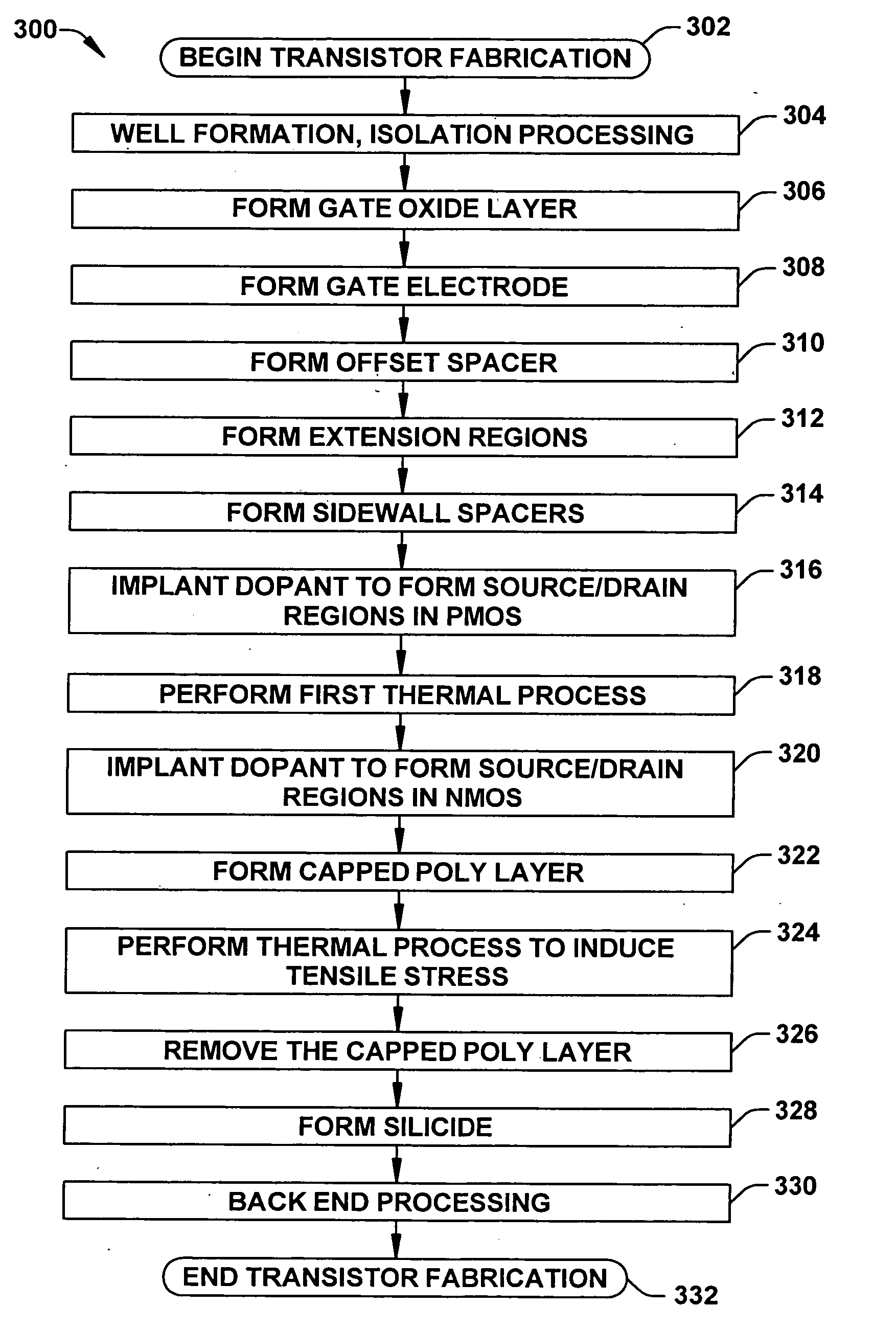
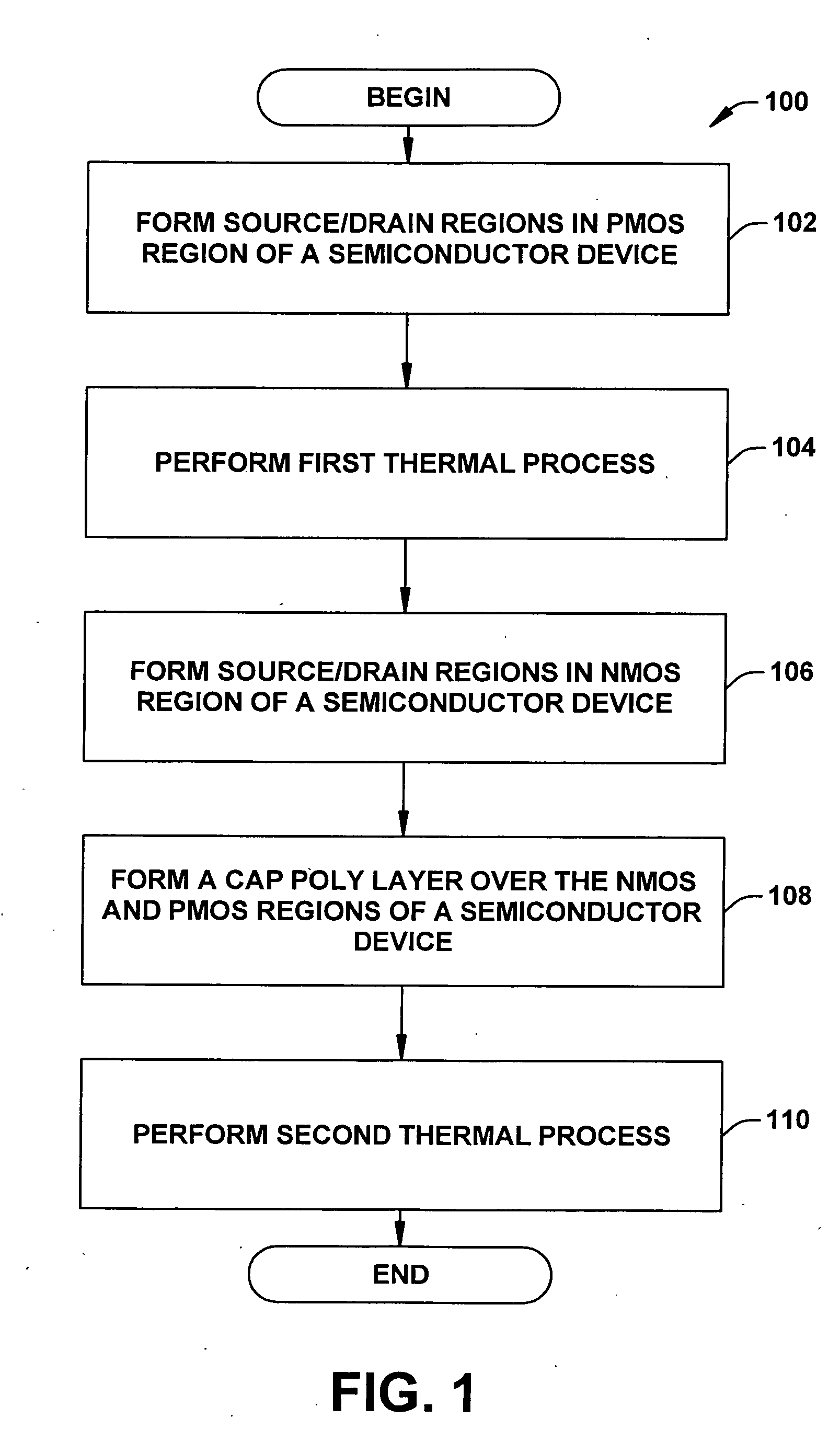
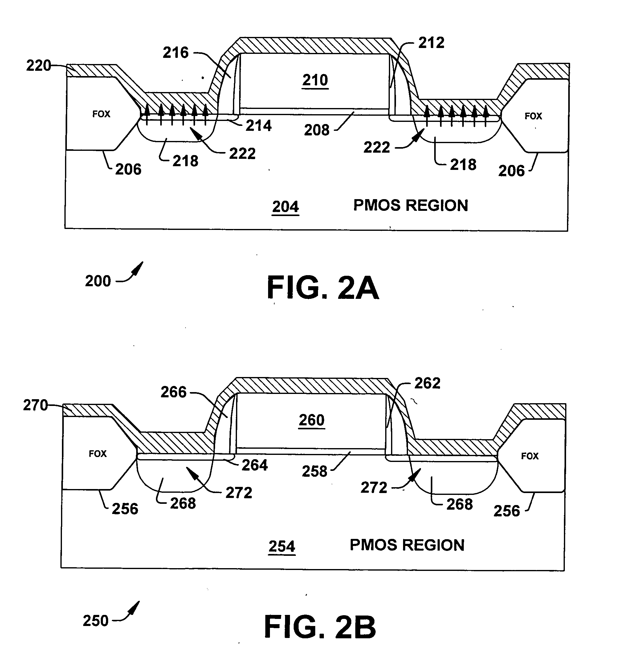
[0016] One or more implementations of the present invention will now be described with reference to the attached drawings, wherein like reference numerals are used to refer to like elements throughout, and wherein the illustrated structures are not necessarily drawn to scale. The invention provides transistor structures and methods in which transistor mobility is improved while reducing masks employed in fabrication thereof.

[0017] The present invention facilitates semiconductor fabrication by providing methods of fabrication that induce stress / strain to channel regions of transistor devices. The present invention forms source / drain regions within a PMOS region followed by a first thermal process that activates the formed source / drain regions and drives in implanted dopants. Afterward, a capped poly layer is formed followed by a strain inducing thermal process that induces stress into channel regions within an NMOS region via the capped poly layer. Unwanted dopant diffusion from the...


PUM


Abstract

The present invention facilitates semiconductor fabrication by providing methods of fabrication that apply tensile strain to channel regions of devices while mitigating unwanted dopant diffusion, which degrades device performance. Source/drain regions are formed in active regions of a PMOS region (102). A first thermal process is performed that activates the formed source/drain regions and drives in implanted dopants (104). Subsequently, source/drain regions are formed in active regions of an NMOS region (106). Then, a capped poly layer is formed over the device (108). A second thermal process is performed (110) that causes the capped poly layer to induce strain into the channel regions of devices. Because of the first thermal process, unwanted dopant diffusion, particularly unwanted p-type dopant diffusion, during the second thermal process is mitigated.

Description

FIELD OF INVENTION [0001] The present invention relates generally to semiconductor devices and more particularly to transistors and associated methods of manufacture having improved mobility due to channel strain. BACKGROUND OF THE INVENTION [0002] A conventional MOS transistor generally includes a semiconductor substrate, such as silicon, having a source, a drain, and a channel positioned between the source and drain. A gate stack composed of a conductive material (a gate conductor), a dielectric layer (a gate oxide), and sidewall spacers, is typically located above the channel. The gate oxide is typically located directly above the channel, while the gate conductor, generally comprised of polycrystalline silicon (polysilicon) material, is located above the gate oxide. The sidewall spacers protect the sidewalls of the gate conductor and define the source and drain placement relative to the gate. [0003] Generally, for a given electric field across the channel of a MOS transistor, th...

Claims


Application Information

Patent Timeline
IPC IPC(8): H01L21/84
CPCH01L21/823807H01L21/823814H01L29/6656H01L29/6659H01L29/7843Y10S438/902
Inventor MEHROTRA, MANOJADAM, LAHIR SHAIKZHAO, SONGNANDAKUMAR, MAHALINGAM
Owner TEXAS INSTR INC
Why Eureka
Try Eureka