

Semiconductor device
a technology of semiconductors and devices, applied in the direction of semiconductor devices, electrical devices, transistors, etc., can solve the problems of extreme small channel mobility, poor quality of the interface between the gate insulating film and the sic, and the effort has not yet succeeded in lowering the on-resistance of the misfet, etc., to achieve the effect of improving the channel mobility
- Summary
- Abstract
- Description
- Claims
- Application Information
AI Technical Summary
Benefits of technology
Problems solved by technology
Method used
Image

Examples
first embodiment
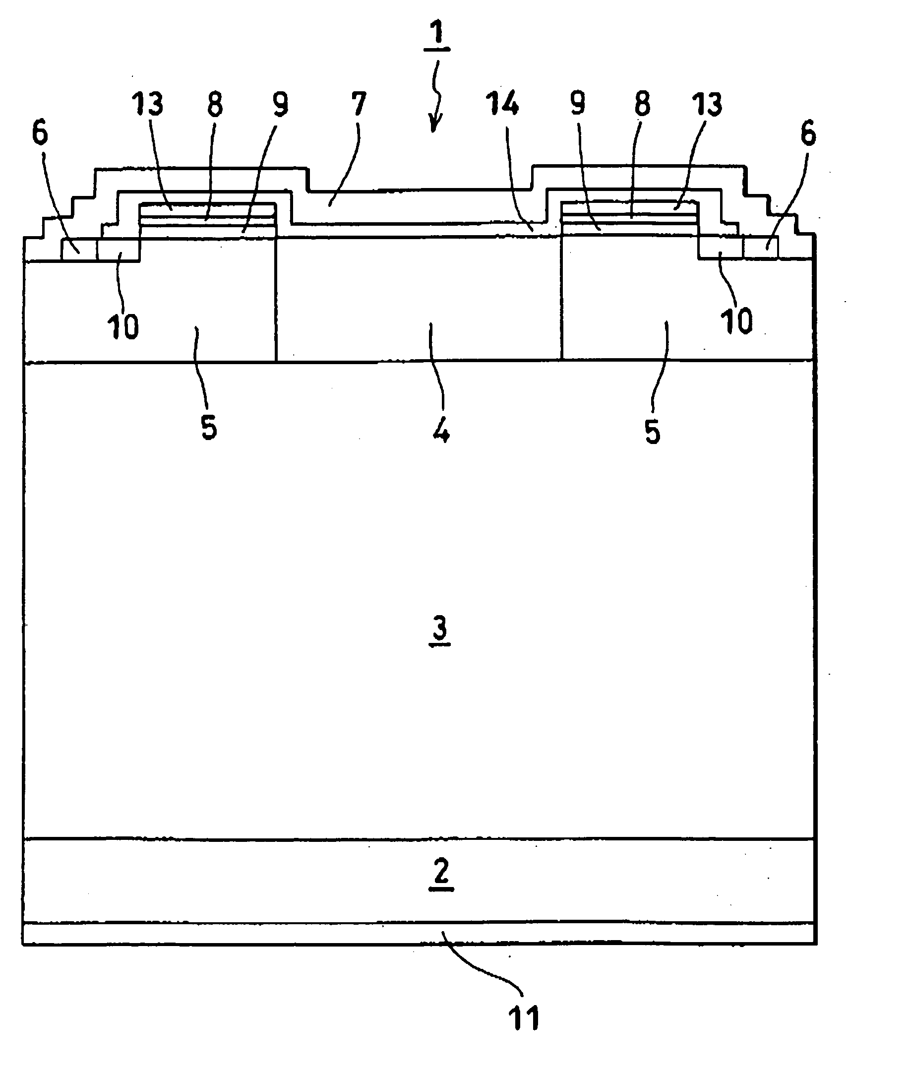
[0025]FIG. 1 is a diagram schematically illustrating a cross section of the semiconductor device according to this invention. With reference to FIG. 1, a semiconductor device 1 is a metal-insulating film-semiconductor field effect transistor (MISFET) of a vertical DMOS structure using a silicon carbide substrate and it is composed of an n-type silicon carbide substrate 2 of a high impurity concentration, an n-type silicon carbide layer 3 of a low impurity concentration disposed thereon, and the individual components superposed thereon.
[0026] Specifically, on the surface of the n-type silicon carbide layer 3, a first n-type silicon carbide region (N− layer) 4 of a first impurity concentration is formed at the center and first p-type silicon carbide regions (p-type (P-)wells) 5, 5 are formed as adjoined respectively to the opposite sides of the first n-type silicon 4.
[0027] Then, in the first p-type silicon carbide regions 5, 5, second n-type silicon carbide regions (N+ sources) 6, 6...
fourth embodiment
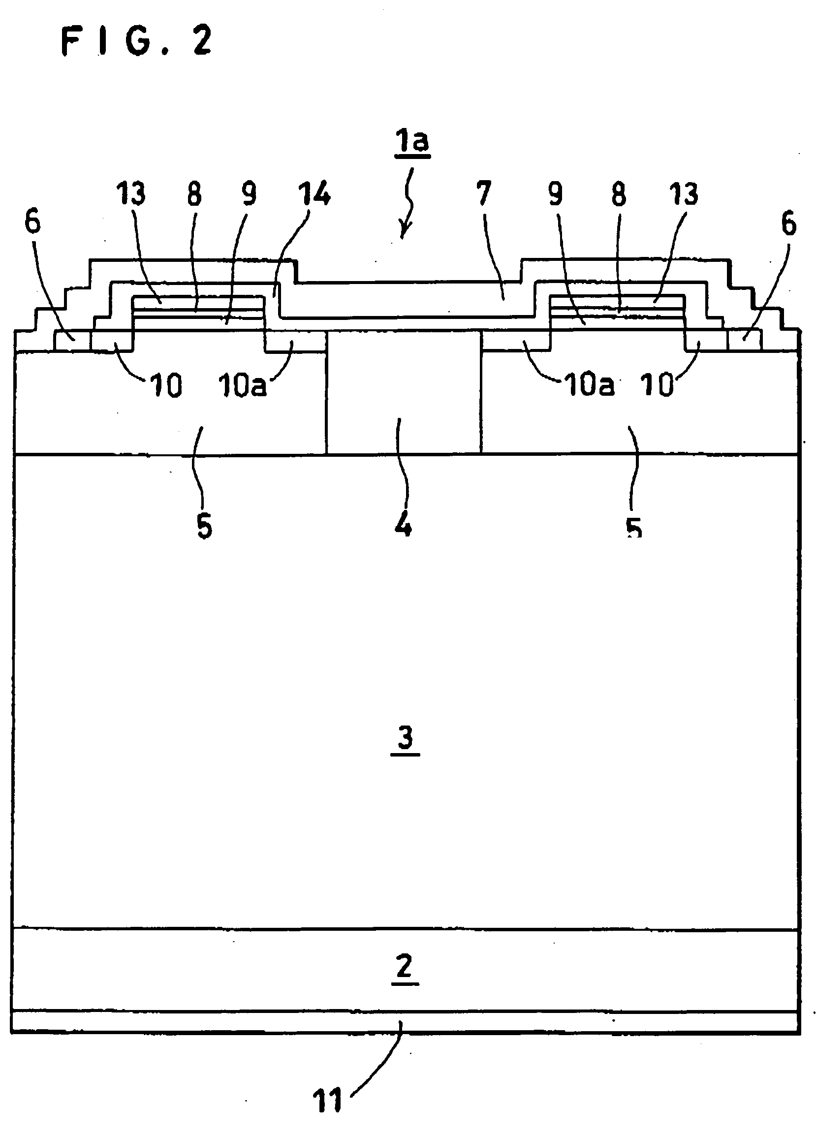
[0039] Now, the process for the production of the semiconductor device 1c of the fourth embodiment will be roughly described below. In this invention, hexagonal silicon carbide or rhombohedral silicon carbide was adopted for the n-type silicon carbide substrate 2 of the high impurity concentration and an n-type silicon carbide layer 3 of a low impurity concentration was formed on the (11-20) face of the hexagonal silicon carbide or rhombohedral silicon carbide.
[0040] Next, on the n-type silicon carbide layer 3, the first n-type silicon carbide region (N− layer) 4 formed of silicon carbide possessing a first impurity concentration was epitaxially grown by the chemical vapor deposition method. Subsequently, the substrate formed of silicon carbide at this stage was given an ordinary RCA cleaning and thereafter an alignment mark for lithography was formed thereon by RIE (reactive ion etching).
[0041] Then, an LTO (low temperature oxide) film was used as a mask for ion implantation. This...
PUM
| Property | Measurement | Unit |
|---|---|---|
| depth | aaaaa | aaaaa |
| thickness | aaaaa | aaaaa |
| depths | aaaaa | aaaaa |
Abstract
Description
Claims
Application Information