Unilateral MOS-type device manufacturing method integrated with SBD structure

A device and range technology, applied in the field of single-side MOS device preparation with integrated SBD structure, can solve the problems of device application cost increase, achieve the effects of reducing the original cell size, improving device conduction ability, and reducing application cost

Inactive Publication Date: 2018-06-19
NO 55 INST CHINA ELECTRONIC SCI & TECHNOLOGYGROUP CO LTD
View PDF7 Cites 21 Cited by
  • Summary
  • Abstract
  • Description
  • Claims
  • Application Information

AI Technical Summary

Problems solved by technology

[0003] In the application of silicon carbide MOSFET devices, it is usually necessary to match a silicon carbide SBD to realize the freewheeling effect, which increases the cost of device application

Method used


Image

  • Unilateral MOS-type device manufacturing method integrated with SBD structure
  • Unilateral MOS-type device manufacturing method integrated with SBD structure
  • Unilateral MOS-type device manufacturing method integrated with SBD structure

Examples


Embodiment Construction

[0021] The technical solutions of the present invention will be further described below in conjunction with the accompanying drawings and embodiments.

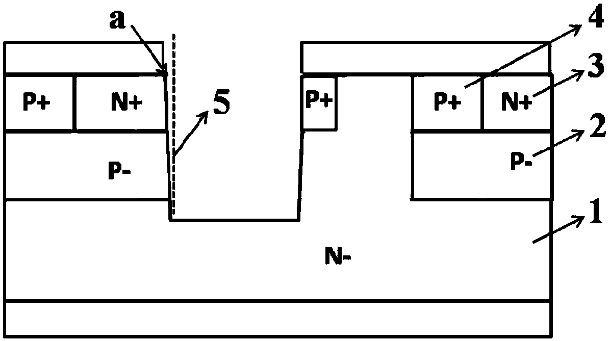
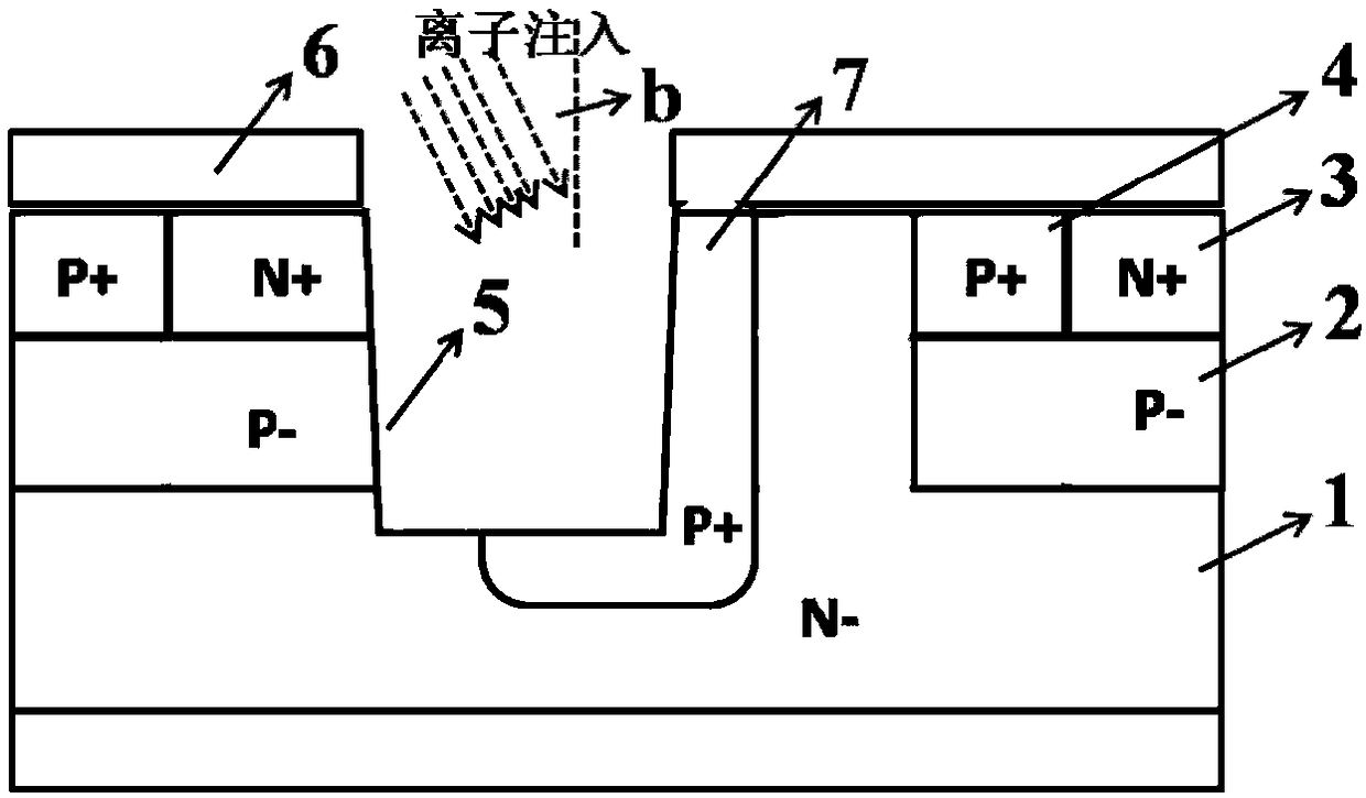
[0022] The present invention provides a novel method for preparing a silicon carbide single-side trench MOS device with an integrated SBD structure through trench etching, oblique angle implantation, front-side ohmic metal and Schottky metal compatible technology, which specifically includes the following steps :

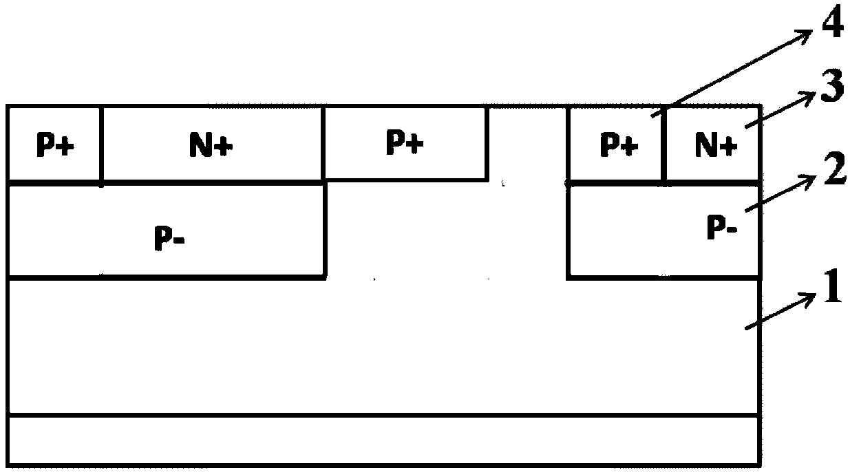
[0023] (1) On the silicon carbide epitaxial layer 1, a plurality of P-Well ion implantation regions 2, N+ ion implantation regions 3, and P+ ion implantation are formed through multiple processes such as growing a dielectric mask, photolithography, etching, and ion implantation Zone 4, such as figure 1 As shown, the doping area, doping concentration and doping distribution can be precisely controlled to realize the substrate material of monolithic integrated silicon carbide MOSFET and SBD structure.

[0024] The i...


PUM

PropertyMeasurementUnit
thicknessaaaaaaaaaa
thicknessaaaaaaaaaa

Abstract

The invention discloses a unilateral MOS-type device manufacturing method integrated with an SBD structure. Through introducing a special angle groove manufacturing process, an inclination angle unilateral ion implantation process and a schottky metal process compatible with an ohm process, manufacturing of an SiC groove MOSFET device integrated with an SBD structure is realized. The silicon carbide SBD structure is integrated in the silicon carbide groove-type MOSFET device, a reverse follow current function can be realized well, the reverse recovery time of the MOSFET device can be reduced,and the application cost of a silicon carbide power electronic device can be effectively reduced. In combination of a unilateral high-mobility groove structure with special crystal face etching, whilethe groove mobility is improved, the size of a primitive cell is narrowed, and the device conduction ability is improved.

Description

technical field [0001] The invention relates to the field of semiconductor devices, in particular to a method for preparing a single-side MOS device with an integrated SBD structure. Background technique [0002] As the third-generation semiconductor material, silicon carbide material has a series of superior properties such as large band gap, high breakdown electric field strength, high saturation drift speed and high thermal conductivity compared with traditional silicon and gallium arsenide materials. Based on the unique material characteristics of silicon carbide materials, it has great application advantages in the fields of high frequency, high power, high voltage and high temperature resistant power electronic devices. In high-end performance switching power supplies, new energy vehicles and rail transit, silicon carbide-based field effect transistor (MOSFET) devices have huge application advantages, which can effectively reduce system size, weight and the demand for ...

Claims


Application Information

Patent Timeline
Patent Type & Authority Applications(China)
IPC IPC(8): H01L29/78H01L21/04
CPCH01L29/66068H01L29/7806H01L29/7813
Inventor 李士颜柏松黄润华刘昊
Owner NO 55 INST CHINA ELECTRONIC SCI & TECHNOLOGYGROUP CO LTD
Why Eureka
Try Eureka