Method for interconnecting back faces of wafer level chips during packaging

A wafer-level chip and backside technology, which is applied in wafer-level chip packaging to form openings exposing solder pads, and in the field of backside interconnection, can solve the problem of small area of ​​connectable lines, weak structure strength of solder pads and metal lines, and electrical continuity. The performance is not reliable enough to achieve the effect of increasing the contact area and improving the circuit conduction performance.

Inactive Publication Date: 2015-04-29
HUATIAN TECH KUNSHAN ELECTRONICS
View PDF3 Cites 6 Cited by
  • Summary
  • Abstract
  • Description
  • Claims
  • Application Information

AI Technical Summary

Problems solved by technology

Removing the barrier material on the pad usually adopts etching method or laser drilling or mechanical cutting, however, using the etching method must mask, which increases the photolithography process; using laser drilling (such as figure 2 When the opening through the pad is formed by mechanical cutting, the opening can only expose the side of the pad, the area that can be connected to the circuit is small, the electrical conduction performance is not reliable enough, and the structural strength between the pad and the metal circuit is also relatively weak. weak

Method used


Image

  • Method for interconnecting back faces of wafer level chips during packaging
  • Method for interconnecting back faces of wafer level chips during packaging
  • Method for interconnecting back faces of wafer level chips during packaging

Examples


Embodiment Construction

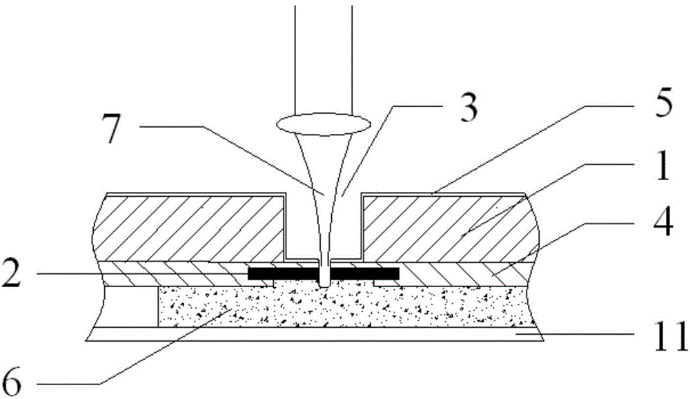
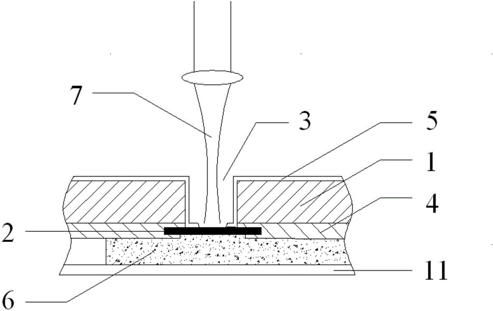
[0038] Such as image 3 , Figure 4 with Figure 5 As shown, a method for forming an opening for exposing the bonding pad 2 in a wafer-level chip package includes the following steps:

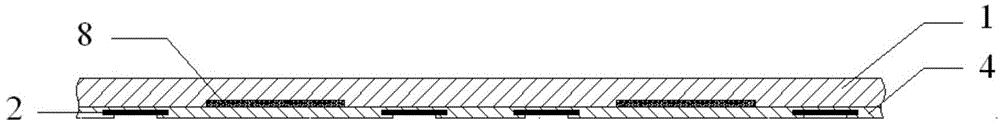
[0039] a. Provide a wafer with several chip units. The chip units include a substrate 1 and a dielectric layer 4 on the front surface of the substrate 1. The front surface of the substrate 1 is provided with a component area 8, and the component area 8 A number of solder pads 2 are provided on the periphery, and the solder pads 2 are located in the dielectric layer 4, and the component area 8 is electrically connected to the solder pads 2 on the periphery;

[0040] b. A first opening 3 opposite to the solder pad 2 is formed on the back of the substrate 1, and the first opening 3 extends from the back of the substrate 1 to above the corresponding solder pad 2;

[0041] c. Laying an insulating layer 5 in the first opening 3 formed in step b and on the back surface of the substrate 1;

[0042] d. Use a l...


PUM


Abstract

The invention discloses a method for interconnecting back faces of wafer level chips during packaging. Blocking materials on a wafer welding cushion are removed through laser etching, a certain area of surface of the welding cushion is exposed to be connected with a metal wiring layer, and electricity of an element area is led to the back faces of wafers. Through the method that the blocking materials on the welding cushion are removed directly through laser etching, the process steps of photoresist coating, photo-etching exposure, developing, photoresist removing and the like are omitted; by selecting an appropriate laser wavelength, adjusting the laser focusing position, adjusting the energy, focus spot area, acting pulse number and other parameters of lasers acting at the bottom of a first opening and controlling laser etching to reach the surface of the welding cushion without penetrating through the welding cushion, a large area of the welding cushion is exposed. The method is convenient to operate, the contact area of the welding cushion and the metal wiring layer is enlarged, and conductivity is more reliable.

Description

Technical field [0001] The present invention relates to a method for wafer-level chip packaging, in particular to a method for forming openings for exposing solder pads in wafer-level chip packaging to realize backside interconnection. Background technique [0002] Such as figure 1 As shown, the general structure of the wafer includes several chip units. Each chip unit includes a substrate 1 and a dielectric layer 4 on the front surface of the substrate. The front surface of the substrate is provided with a component area 8, and the periphery of the component area is provided with several The soldering pad 2 is located in the dielectric layer, and the component area is electrically connected to the surrounding soldering pads; in this structure, the soldering pad and the substrate are separated by dielectric material. At present, the TSV packaging steps of wafer-level chips include making an opening on the back of the wafer substrate, which extends from the back of the wafer to th...

Claims


Application Information

Patent Timeline
Patent Type & Authority Applications(China)
IPC IPC(8): H01L21/768
CPCH01L21/76898
Inventor 谷成进万里兮范俊廖建亚黄小花翟玲玲钱静娴
Owner HUATIAN TECH KUNSHAN ELECTRONICS
Why Eureka
Try Eureka