Layout method of SiC JBS device

A layout method and device technology, which are applied in the manufacture of electrical solid-state devices, semiconductor devices, semiconductor/solid-state devices, etc., can solve the problem of affecting the pinch-off ability of Schottky junctions, the strip structure is difficult to achieve uniformity, and it cannot effectively reduce the size of the To solve the problems such as the electric field on the surface of the Teky, to increase the contact area of ​​the Schottky, increase the area of ​​the Schottky barrier area, and ensure the reverse breakdown characteristics.

Pending Publication Date: 2020-06-09
GLOBAL ENERGY INTERCONNECTION RES INST CO LTD
View PDF0 Cites 6 Cited by
  • Summary
  • Abstract
  • Description
  • Claims
  • Application Information

AI Technical Summary

Problems solved by technology

At present, in order to increase the conduction current of the device, the way of multi-cell parallel connection is usually adopted. Different cell shapes and layouts will affect the breakdown voltage and on-resistance, but the common square array, because the diagonal P+ area spacing is greater than The distance between adjacent P+ regions cannot effectively reduce the Schottky surface electric field in the middle region, which affects the pinch-off ability of the Schottky junction during reverse bias; and the strip structure is difficult to achieve ideal uniformity in terms of processing technology , so it is worth studying to provide a SiC JBS device that is easy to implement and has high precision in the process

Method used


Image

  • Layout method of SiC JBS device
  • Layout method of SiC JBS device
  • Layout method of SiC JBS device

Examples


Embodiment 1

[0056] The purpose of the present invention is to provide a SiC JBS device, which mainly lies in the arrangement of the P-type region in the active region. Compared with the traditional layout method, while ensuring the reverse blocking voltage of the device, it increases the Schottke as much as possible. The area of ​​the base contact area is small, and the process is easy to realize, achieving a reasonable compromise between breakdown voltage, on-resistance characteristics and process difficulty.

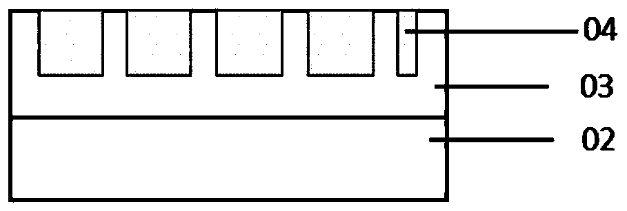
[0057] an active area and a terminal protection area, the terminal protection area is arranged around the active area, and the active area includes a plurality of P-type areas and Schottky contact areas; the active area is a rectangular structure;

[0058] The multiple P-type regions are arranged alternately in multiple rows and columns, and the Schottky contact regions are filled between the P-type regions.

[0059] The P-type region includes a complete P-type region and a half-P...

Embodiment 2

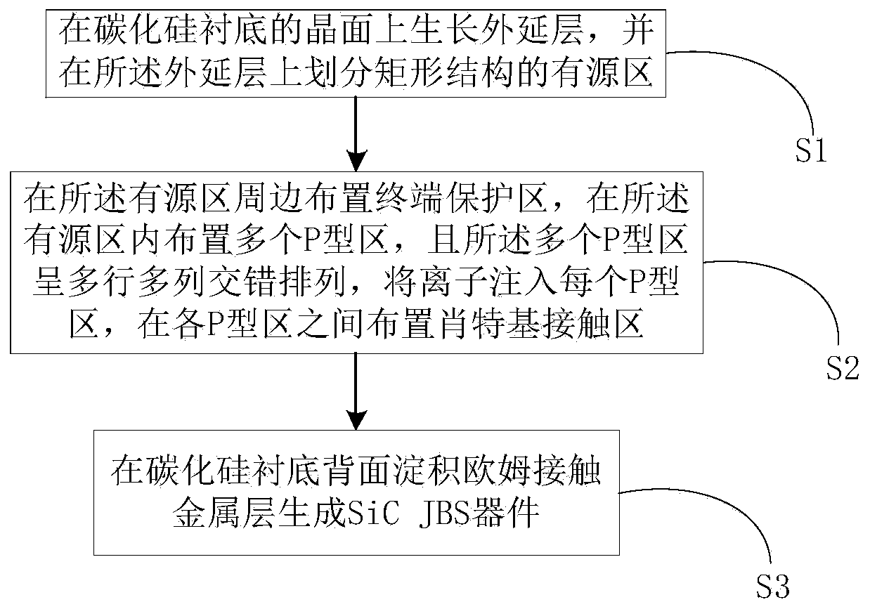
[0070] Based on the same inventive concept, this embodiment also provides a layout method for SiC JBS devices, which is suitable for manufacturing processes, such as figure 1 shown, including:

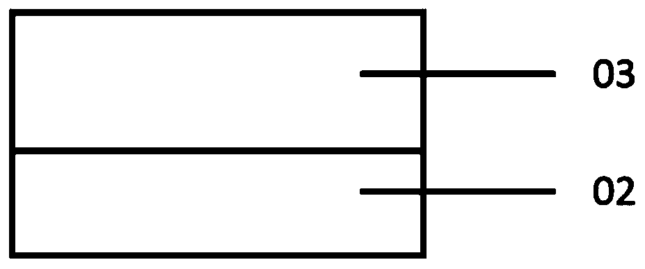
[0071] Step S1, growing an epitaxial layer on the crystal plane of the silicon carbide substrate, and dividing an active region of a rectangular structure on the epitaxial layer;

[0072] Step S2, arranging a plurality of P-type regions in the active region, and the plurality of P-type regions are arranged alternately in multiple rows and columns, implanting ions into each P-type region, and arranging between the P-type regions Schottky contact area;

[0073] Step S3, depositing an ohmic contact metal layer on the back surface of the silicon carbide substrate to form a SiC JBS device.

[0074] The specific layout methods of SiC JBS devices include:

[0075] Step S1, growing an epitaxial layer on the crystal plane of the silicon carbide substrate, and dividing an active region of a r...


PUM

PropertyMeasurementUnit
electrical resistivityaaaaaaaaaa
thicknessaaaaaaaaaa
thicknessaaaaaaaaaa

Abstract

The invention provides a layout method of a SiC JBS device, which comprises the following steps of: growing an epitaxial layer on the crystal surface of a silicon carbide substrate, and dividing an active region with a rectangular structure on the epitaxial layer, arranging a terminal protection region at the periphery of the active region, arranging a plurality of P-type regions in the active region, arranging the plurality of P-type regions in a multi-row and multi-column staggered manner, implanting ions into each P-type region, and arranging Schottky contact regions between the P-type regions, and depositing an ohmic contact metal layer on the back surface of the silicon carbide substrate to generate the SiC JBS device. The plurality of P-type regions are arranged in the SiC JBS devicein a multi-row and multi-column staggered manner, so that the reverse breakdown characteristic of the SiC JBS device is ensured, the Schottky barrier region area is increased, and the conduction capability is improved.

Description

technical field [0001] The invention relates to the field of semiconductor devices and their manufacture, in particular to a layout method for SiC JBS devices. Background technique [0002] High-power diodes are an important branch of semiconductor power electronic devices, mainly including Schottky Barrier Diodes (Schottky Barrier Diode, SBD), Junction Barrier Schottky Diodes (JBS), and PiN diodes. In the field of silicon carbide (SiC) with high voltage and high current, SiC SBD diodes are widely used due to their low forward voltage drop, but the existence of Schottky barriers makes the reverse leakage current of SBD diodes relatively large, limiting for its high-voltage applications. Although the SiC PiN diode has a high blocking voltage, due to the conductance modulation effect, the energy loss of the SiC PiN diode is relatively large during reverse recovery. [0003] Therefore, in order to solve the above problems, the junction barrier Schottky diode structure is usua...

Claims


Application Information

Patent Timeline
Patent Type & Authority Applications(China)
IPC IPC(8): H01L29/872H01L27/02H01L21/329H01L29/16
CPCH01L27/0207H01L29/1608H01L29/6606H01L29/872
Inventor 杨霏张文婷田丽欣夏经华吴沛飞
Owner GLOBAL ENERGY INTERCONNECTION RES INST CO LTD
Why Eureka
Try Eureka