Unlock instant, AI-driven research and patent intelligence for your innovation.
SiC JBS device
What is Al technical title?
Al technical title is built by PatSnap Al team. It summarizes the technical point description of the patent document.
A device and consistent technology, applied in the field of SiCJBS devices, to ensure the reverse breakdown characteristics, increase the Schottky contact area, and increase the area of the effect
Pending Publication Date: 2020-06-09
GLOBAL ENERGY INTERCONNECTION RES INST CO LTD
View PDF0 Cites 0 Cited by
Summary
Abstract
Description
Claims
Application Information
AI Technical Summary
This helps you quickly interpret patents by identifying the three key elements:
Problems solved by technology
Method used
Benefits of technology
Problems solved by technology
[0005] In order to solve the problem of effective shielding of the Schottky junction by the depletion layer during reverse bias in the prior art
Method used
Image
Click on the blue label to locate the original text in one second.
Reading with bidirectional positioning of images and text.
Examples
Embodiment 1
[0056] The purpose of the present invention is to provide a SiC JBS device, which mainly lies in the arrangement of the P-type region in the active region. Compared with the traditional layout method, while ensuring the reverse blocking voltage of the device, it increases the Schottke as much as possible. The area of the base contact area is small, and the process is easy to realize, achieving a reasonable compromise between breakdown voltage, on-resistance characteristics and process difficulty.
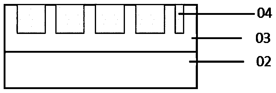
[0057] an active area and a terminal protection area, the terminal protection area is arranged around the active area, and the active area includes a plurality of P-type areas and Schottky contact areas; the active area is a rectangular structure;
[0058] The multiple P-type regions are arranged alternately in multiple rows and columns, and the Schottky contact regions are filled between the P-type regions.
[0059] The P-type region includes a complete P-type region and a half-P...
Embodiment 2
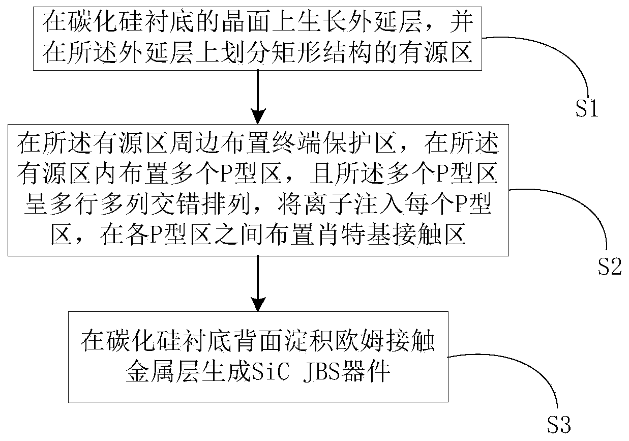
[0070] Such as figure 1 As shown, based on the same inventive concept, this embodiment also provides a layout method for SiC JBS devices, which is suitable for the manufacturing process, including:
[0071] Step S1, growing an epitaxial layer on the crystal plane of the siliconcarbide substrate, and dividing an active region of a rectangular structure on the epitaxial layer;
[0072] Step S2, arranging a terminal protection area around the active region, arranging a plurality of P-type regions in the active region, and the plurality of P-type regions are arranged in multiple rows and columns, and implanting ions into each P-type regions, Schottky contact regions are arranged between the P-type regions;
[0073] Step S3, depositing an ohmic contactmetal layer on the back surface of the siliconcarbide substrate to form a SiC JBS device.
[0074] The specific layout methods of SiC JBS devices include:
[0075] Step S1, growing an epitaxial layer on the crystal plane of the ...
PUM
Property
Measurement
Unit
electrical resistivity
aaaaa
aaaaa
thickness
aaaaa
aaaaa
thickness
aaaaa
aaaaa
Abstract
The invention provides a SiC JBS device, which comprises an active region and a terminal protection region, wherein the terminal protection region is arranged at the periphery of the active region, and the active region comprises a plurality of P-type regions and Schottky contact regions; the active region is of a rectangular structure; the plurality of P-type regions are arranged in a multi-row and multi-column staggered manner; and the Schottky contact regions are filled among the P-type regions. The plurality of P-type regions provided by the invention are arranged in a multi-row and multi-column staggered manner, so that the reverse breakdown characteristic of the SiC JBS device is ensured, the Schottky barrier region area is increased, and the conduction capability is improved.
Description
technical field [0001] The invention relates to the field of semiconductor devices and their manufacture, in particular to a SiC JBS device. Background technique [0002] High-power diodes are an important branch of semiconductor power electronic devices, mainly including Schottky Barrier Diodes (Schottky BarrierDiode, SBD), Junction Barrier Schottky Diodes (JBS), and PiN diodes. In the field of siliconcarbide (SiC) with high voltage and high current, SiC SBD diodes are widely used due to their low forward voltage drop, but the existence of Schottky barriers makes the reverse leakage current of SBD diodes relatively large, limiting for its high-voltage applications. Although the SiC PiN diode has a high blocking voltage, due to the conductance modulation effect, the energy loss of the SiC PiN diode is relatively large during reverse recovery. [0003] Therefore, in order to solve the above problems, the junction barrier Schottky diode structure is usually adopted interna...
Claims
Application Information
Patent Timeline
Application Date:The date an application was filed.
Publication Date:The date a patent or application was officially published.
First Publication Date:The earliest publication date of a patent with the same application number.
Issue Date:Publication date of the patent grant document.
PCT Entry Date:The Entry date of PCT National Phase.
Estimated Expiry Date:The statutory expiry date of a patent right according to the Patent Law, and it is the longest term of protection that the patent right can achieve without the termination of the patent right due to other reasons(Term extension factor has been taken into account ).
Invalid Date:Actual expiry date is based on effective date or publication date of legal transaction data of invalid patent.
Patent Type & Authority Applications(China)
IPC IPC(8): H01L29/872H01L27/02H01L21/329
CPCH01L29/872H01L27/0207H01L29/6606
Inventor 张文婷杨霏郑柳桑玲焦倩倩夏经华田丽欣吴沛飞
Owner GLOBAL ENERGY INTERCONNECTION RES INST CO LTD

