Semiconductor device and manufacturing method thereof

a technology of semiconductors and semiconductors, applied in the direction of semiconductor devices, basic electric elements, electrical appliances, etc., can solve the problems of corresponding decrease in carrier mobility, and have not been verified yet whether or not, and achieve the effect of reducing contact resistan

Active Publication Date: 2014-04-24
SEMICON MFG INT (SHANGHAI) CORP
View PDF5 Cites 22 Cited by
  • Summary
  • Abstract
  • Description
  • Claims
  • Application Information

AI Technical Summary

Benefits of technology

[0024]In some embodiments, the method of manufacturing the semiconductor device may include depositing a barrier layer between the work function material layer and the gate metal, removing a portion of the work function material layer, the barrier layer, and

Problems solved by technology

However, a reduction in MOSFET size also leads to a corresponding decrease in carrier mobility.
However, currently it has not been verified

Method used


Image

  • Semiconductor device and manufacturing method thereof
  • Semiconductor device and manufacturing method thereof
  • Semiconductor device and manufacturing method thereof

Examples


Embodiment Construction

[0034]In the present disclosure, the term “semiconductor device” refers to a device having one or more semiconductor materials. The device may include a manufactured semiconductor device product and / or an intermediate semiconductor device product formed during a manufacturing or machining process.

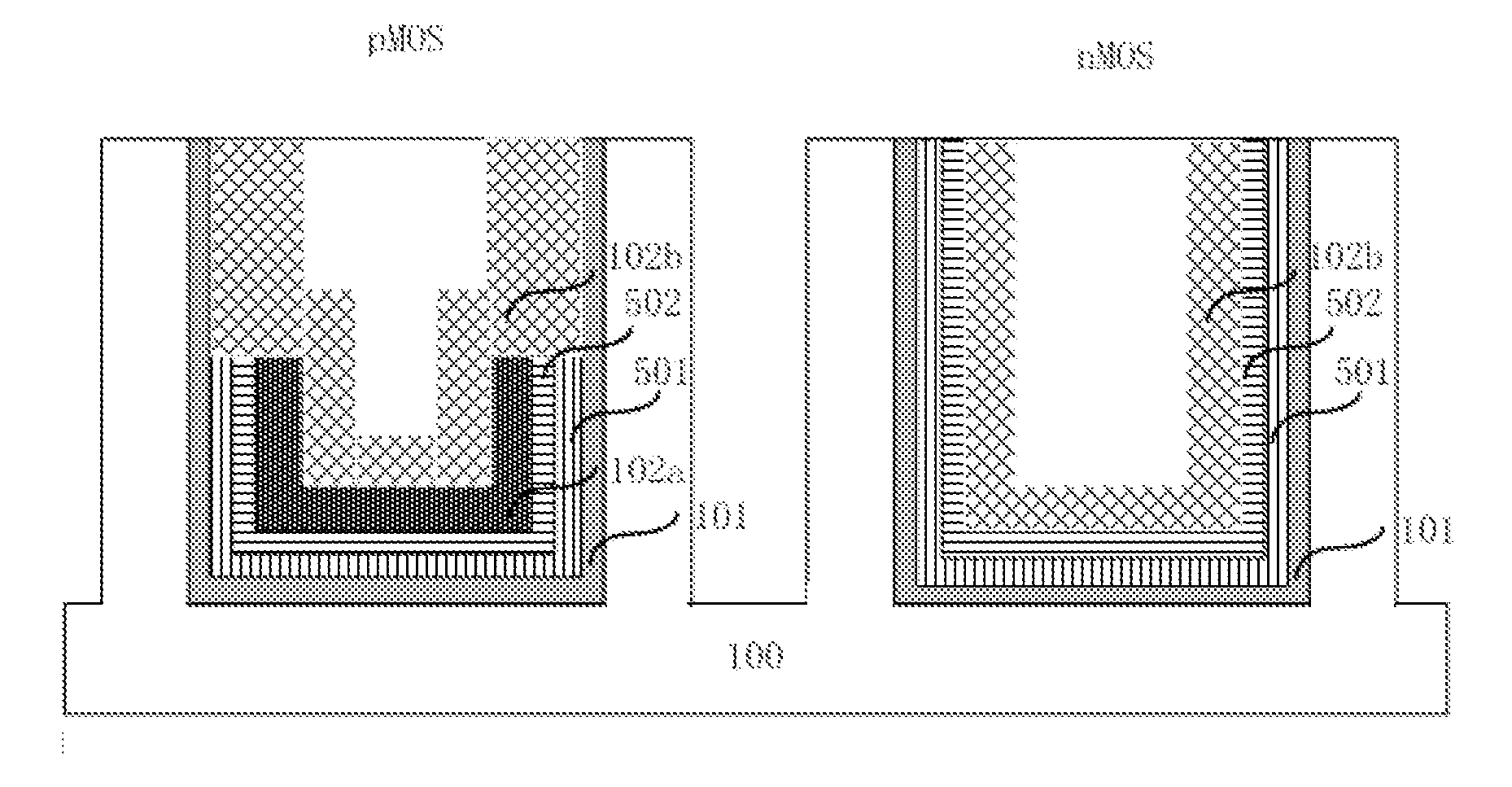
[0035]FIG. 1 shows a cross-sectional view of a semiconductor device according to an embodiment of the present disclosure.

[0036]As shown in FIG. 1, the semiconductor device includes a gate insulating layer 101 formed on an inner wall of a recess 104 of a substrate 100, a work function material layer 102 formed on the gate insulating layer 101, and a gate metal 106 formed on the work function material layer 102 and filling the recess 104. The gate insulating layer 101, the work function material layer 102, and the gate metal 106 may be formed in the order as stated above.

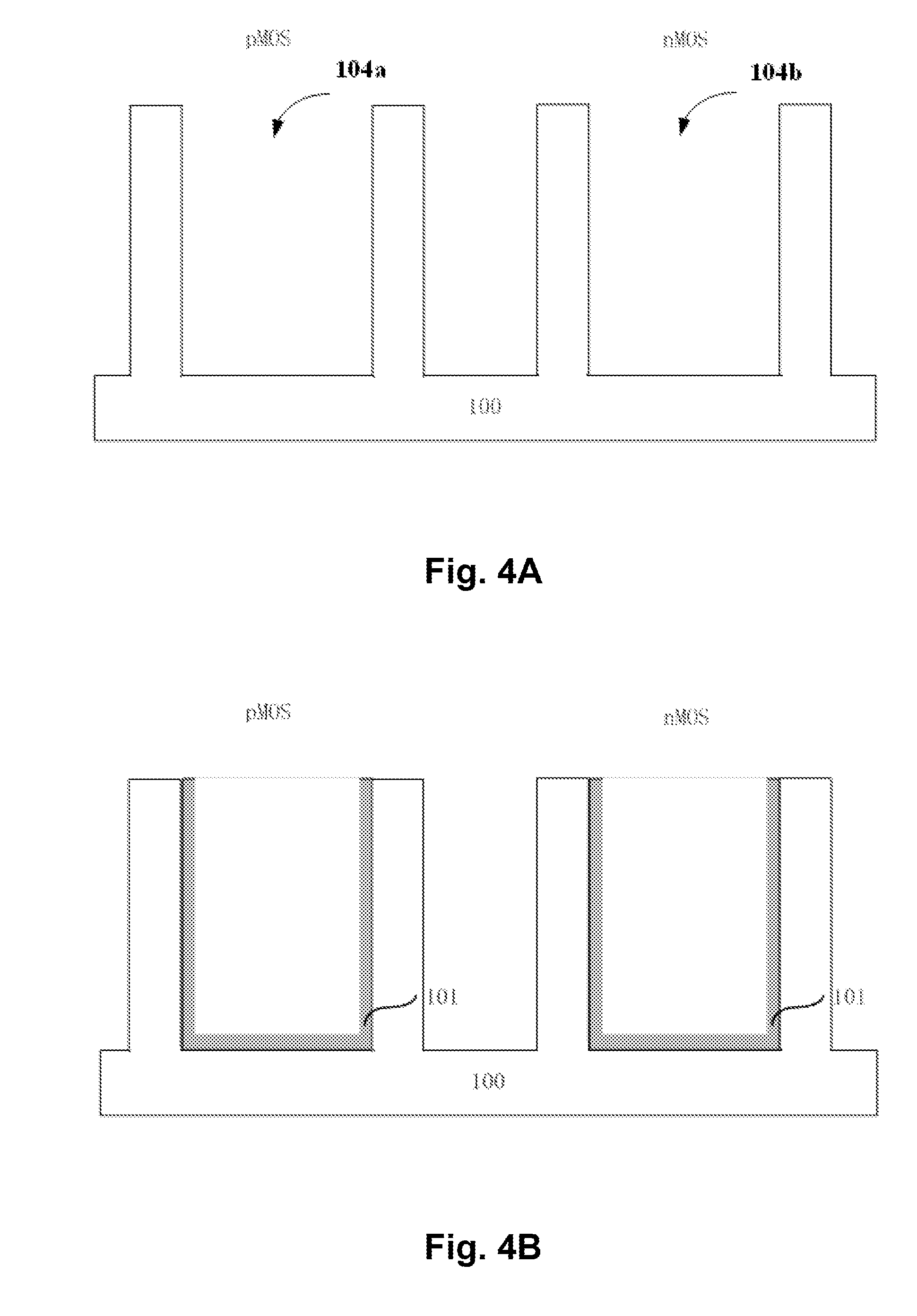
[0037]The recess 104 may be, for example, a recess formed in the substrate 100 after removal of a dummy gate previously for...


PUM


Abstract

The present invention discloses a semiconductor device and a method for manufacturing the semiconductor device. The semiconductor device includes a gate insulating layer formed on an inner wall of a substrate recess, a work function material layer formed on the gate insulating layer so as to apply a tensile stress or a compressive stress to a channel of a MOS field-effect transistor, and a gate metal formed on the work function material layer. The method for manufacturing the semiconductor device includes forming a work function material layer on a gate insulating layer so as to apply a tensile stress or a compressive stress to a channel of a MOS field-effect transistor, wherein the gate insulating layer is formed on an inner wall of a substrate recess, and depositing a gate metal on the work function material layer.

Description

CROSS-REFERENCE TO RELATED APPLICATIONS[0001]This application claims priority to Chinese Patent Application No. 201210398918.7 filed with SIPO on Oct. 19, 2012 and entitled “Semiconductor Device and Manufacturing Method thereof”, which is incorporated herein by reference in its entirety.FIELD OF THE INVENTION[0002]The present disclosure relates to the field of semiconductor technology, and more particularly to a semiconductor device and method for manufacturing the same.DESCRIPTION OF THE RELATED ART[0003]Advance developments in the field of semiconductor technology have resulted in continuous reductions in the size of the MOSFET (Metal-Oxide-Semiconductor Field-Effect Transistor). However, a reduction in MOSFET size also leads to a corresponding decrease in carrier mobility. The issue of decreased carrier mobility has attracted significant attention in the semiconductor industry, and numerous techniques for increasing the carrier mobility of MOSFETs have been proposed.[0004]In some...

Claims


Application Information

Patent Timeline
IPC IPC(8): H01L29/423H01L29/40
CPCH01L29/401H01L29/4236H01L21/28088H01L21/823842H01L29/4966H01L29/66477H01L29/78H01L21/823807H01L29/66795H01L29/7845H01L29/785
Inventor FUMITAKE, MIENO
Owner SEMICON MFG INT (SHANGHAI) CORP
Why Eureka
Try Eureka