Semiconductor device and manufacturing process therefor

a technology of semiconductor devices and manufacturing processes, applied in semiconductor devices, semiconductor/solid-state device details, electrical apparatus, etc., can solve the problems of defective deposition, ineffective reduction of contact resistance of silicide film on the lateral side, and inability to form silicide films, etc., to achieve easy alignment, easy alignment, and more effective reduction of parasitic resistance

Inactive Publication Date: 2007-04-05
NEC CORP
View PDF7 Cites 90 Cited by
  • Summary
  • Abstract
  • Description
  • Claims
  • Application Information

AI Technical Summary

Benefits of technology

[0044] Preferably, the semiconductor device of this invention further comprising a planar type field effect transistor having a semiconductor region on whose upper surface a main channel is formed, and an elevated source / drain region.
[0045] This invention can provide a semiconductor device having a fin-type MISFET, which has a slope or a concavity and convexity portion in a source / drain region whereby a contact resistance is reduced and a contact hole can be easily aligned, as well as a process for manufacturing such a device.
[0046] In this invention, there is made a slope or a concavity and convexity portion where a silicide film is formed over the whole surface of the source / drain region, so that the silicide film is allowed to be formed in a larger area. As a result, a contact hole can be more easily aligned and a parasitic resistance can be more effectively reduced.
[0047] In this invention, there is a plane parallel with a substrate plane in the uppermost side in a source / drain region, which allows a thicker suicide film to be formed, resulting in more effective reduction of a parasitic resistance.
[0048] In this invention, a multi-structural MISFET may have s source / drain region having a slope or a concavity and convexity portion, which allows a silicide film to be formed in a larger area and facilitates alignment of a contact hole in comparison with a single-structural MISFET.

Problems solved by technology

However, a fin-type MISFET described in patent references 1 to 3 has a substantially cuboid source / drain region whose lateral sides are mainly perpendicular to a substrate, so that the silicide film cannot be formed on the lateral sides by sputtering.
If CVD is used to form a silicide film on the lateral sides, it may lead to defective deposition such as facet formation or the whole source / drain region may be silicided.
Thus, silicide formation may not effectively reduce a contact resistance.
It, therefore, becomes difficult to align a contact hole with a source / drain region in the MISFET.

Method used


Image

  • Semiconductor device and manufacturing process therefor
  • Semiconductor device and manufacturing process therefor
  • Semiconductor device and manufacturing process therefor

Examples


embodiment 1

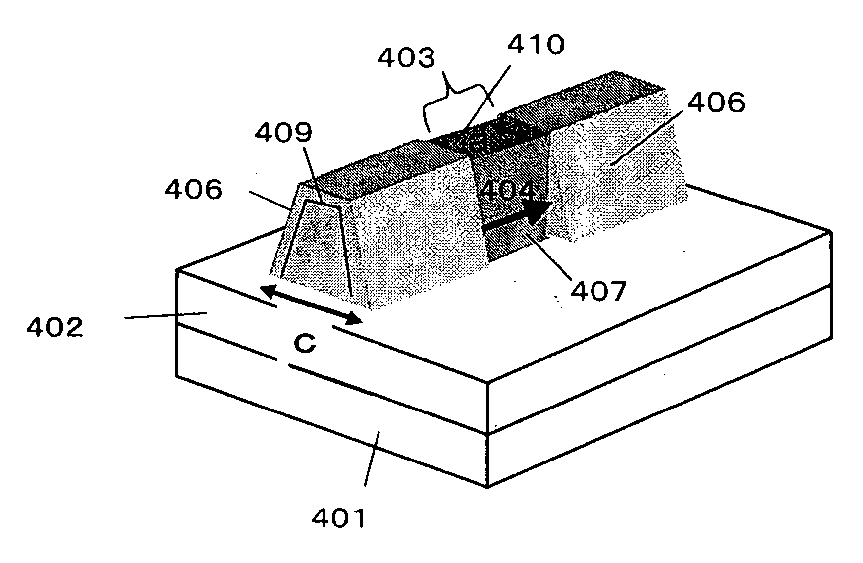
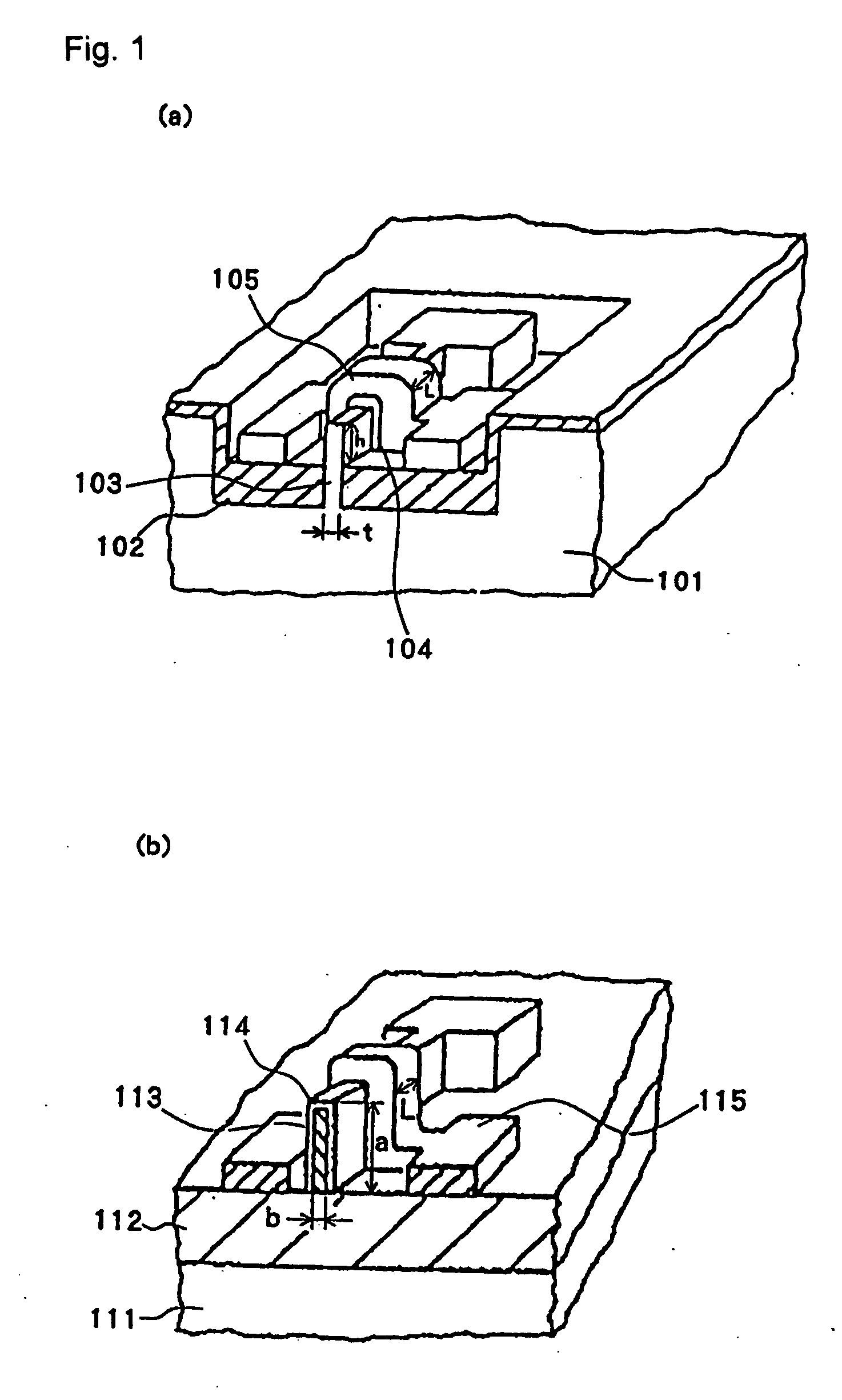
[0098] The first embodiment of this invention relates to a semiconductor device having a single-structural fin-type MISFET. A single-structural MISFET has a protruding semiconductor region and a paired source / drain region within one transistor.

[0099] The source / drain region in this embodiment may have various shapes as shape of slope as long as the source / drain region has a slope in which at least the largest width is larger than a width of the semiconductor region and width continuously increases from the uppermost side to the substrate side.

[0100] The slope of the source / drain region may be, for example, a curve where a width increases from the uppermost side to the substrate side at an inconstant rate or a taper where a width increases at a constant rate.

[0101]FIG. 5(a) is a plan view of a semiconductor device having an MISFET in which a source / drain region is tapered. FIG. 5(b) is a cross-sectional view of the semiconductor device taken on line A-A in FIG. 5(a), and FIG. 5(c)...

embodiment 2

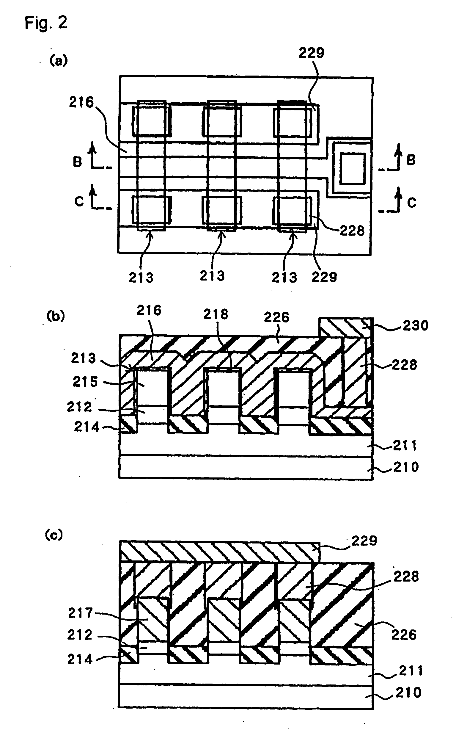
[0111] The second embodiment of this invention relates to a semiconductor device having a multi-structural MISFET. A multi-structural MISFET has a configuration where within one transistor, a plurality of protruding semiconductor regions are aligned in parallel in a direction perpendicular to a channel current flow direction and a gate electrode 501 is a conductor interconnection striding over the plurality of protruding semiconductor regions.

[0112] FIGS. 9(a) and 10(a) are plan views of a semiconductor device having an MISFET. FIGS. 9(b) and 10(b) are cross-sectional view of the semiconductor devices taken on line B-B in FIGS. 9(a) and 10(a), respectively. FIGS. 9(c) and 10(c) are cross-sectional views of the semiconductor devices taken on line A-A in FIGS. 9(a) and FIG. 10(a), respectively.

[0113] In the MISFET in FIG. 9, a plurality of protruding semiconductor regions 506 (only two in this figure) are disposed in a direction 517 perpendicular to a channel current flow direction,...


PUM


Abstract

There is provided a semiconductor device wherein at least the largest width of a source/drain region is larger than the width of a semiconductor region and the source/drain region has a slope having a width continuously increasing from the uppermost side to the substrate side, and a silicide film is formed in the surface of the slope.

Description

TECHNICAL FIELD [0001] This invention relates to a semiconductor device having a fin-type field effect transistor with a lower contact resistance in which a contact hole can be easily aligned. BACKGROUND OF THE INVENTION [0002] There has been developed a fin-type MIS type field effect transistor (hereinafter, referred to as “MISFET”) having a protrusion consisting of a semiconductor region in which a main channel is formed in planes (lateral sides of the protrusion) substantially perpendicular to a substrate. A fin-type MISFET is known to be advantageous in terms of size reduction as well as improvement in various properties such as improvement in cutoff properties or carrier mobility and reduction in short channel effect and punch-through. [0003] Japanese Patent Application No. 1989-8670 has disclosed a fin-type MISFET in which a part of a cuboid semiconductor is a part of a silicon wafer substrate and a fi-type MISFET in which a part of a cuboid semiconductor is a part of a monocr...

Claims


Application Information

Patent Timeline
Patent Type & Authority Applications(United States)
IPC IPC(8): H01L23/62H01L21/336H01L29/786
CPCH01L29/42392H01L29/66795H01L29/7853H01L29/7854H01L2924/0002H01L2924/00
Inventor TERASHIMA, KOICHITAKEUCHI, KIYOSHIYAMAGAMI, SHIGEHARUWAKABAYASHI, HITOSHIOGURA, ATSUSHIWATANABE, KOJITATSUMI, TORUTAKEDA, KOICHINOMURA, MASAHIROTANAKA, MASAYASU
Owner NEC CORP
Why Eureka
Try Eureka