Hybrid optical/electronic structures fabricated by a common molding process

a technology of optical/electronic structures and molding processes, applied in the field of can solve the problems of not being able to fully take advantage of the precision alignment design into the mpo interface, and achieve the effect of improving the fabrication of micro lens elements

Inactive Publication Date: 2008-06-24
INT BUSINESS MASCH CORP
View PDF9 Cites 184 Cited by
  • Summary
  • Abstract
  • Description
  • Claims
  • Application Information

AI Technical Summary

Benefits of technology

[0013]Another object of this invention is to fabricate MPO compatible interfaces directly on silicon or other semiconductor chip substrates, making it possible to integrate photodetectors or other active devices with the MPO interface at a chip level.
[0016]The preferred embodiment of the invention, described below in detail, provides a glass micro lens array fabricated using wafer scale manufacturing approaches, because of its superior thermal performance and low manufacturing cost; however, plastic materials may be used as an alternate embodiment. To further reduce the assembly cost, a receptacle may be used that incorporates both an interface for MT array connector and an interface for micro-optics. To facilitate passive alignment between the lens array and fiber array receptacle, mechanical structures may be fabricated on one side of the lens array, which will mate with a precision molded cavity on the receptacle. Also, a release layer may be applied to conformally coat the sidewalls of the cavities in which the micro lenses are formed to help release those formed lenses from the cavities.

Problems solved by technology

Current designs fabricate the MPO connector interface and coupling lenses as separate processes and manually assemble them into a finished product; this requires active alignment (often an expensive, manual process) and cannot fully take advantage of the precision alignment designed into the MPO interface.

Method used


Image

  • Hybrid optical/electronic structures fabricated by a common molding process
  • Hybrid optical/electronic structures fabricated by a common molding process
  • Hybrid optical/electronic structures fabricated by a common molding process

Examples


Embodiment Construction

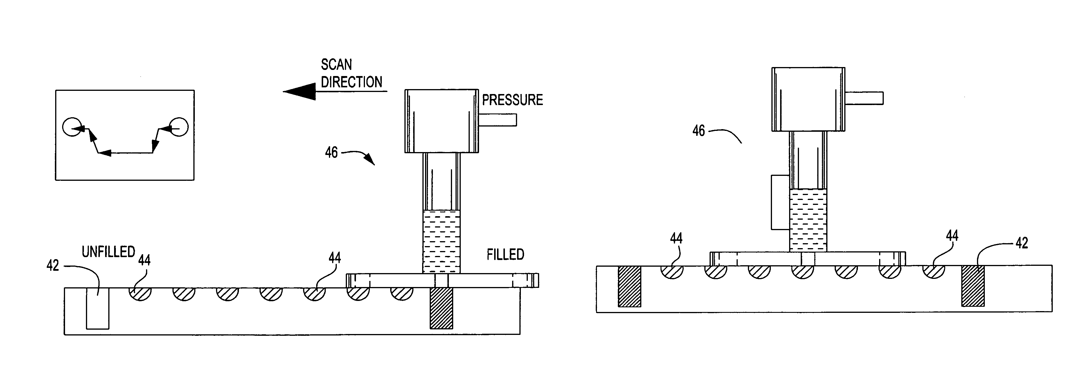
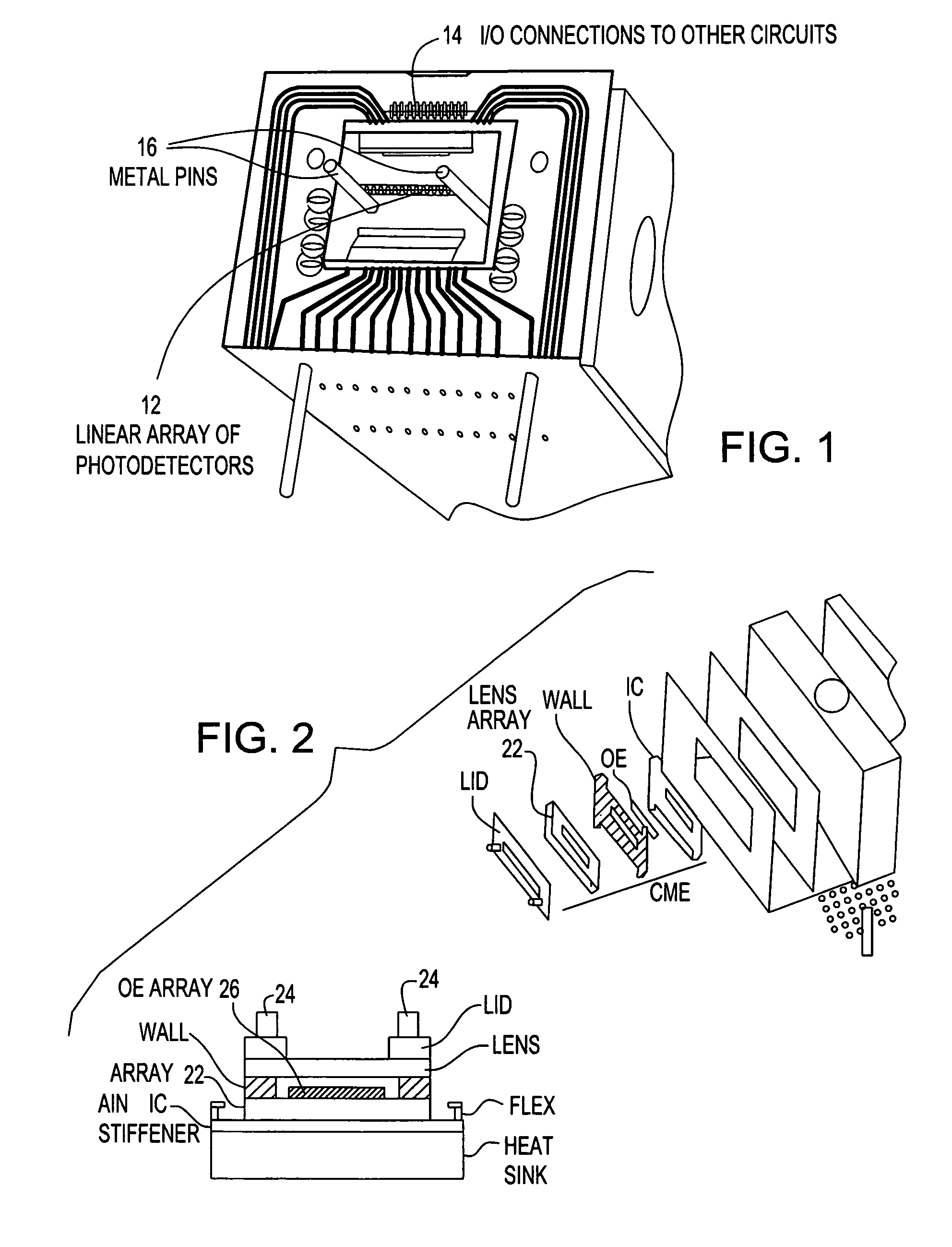
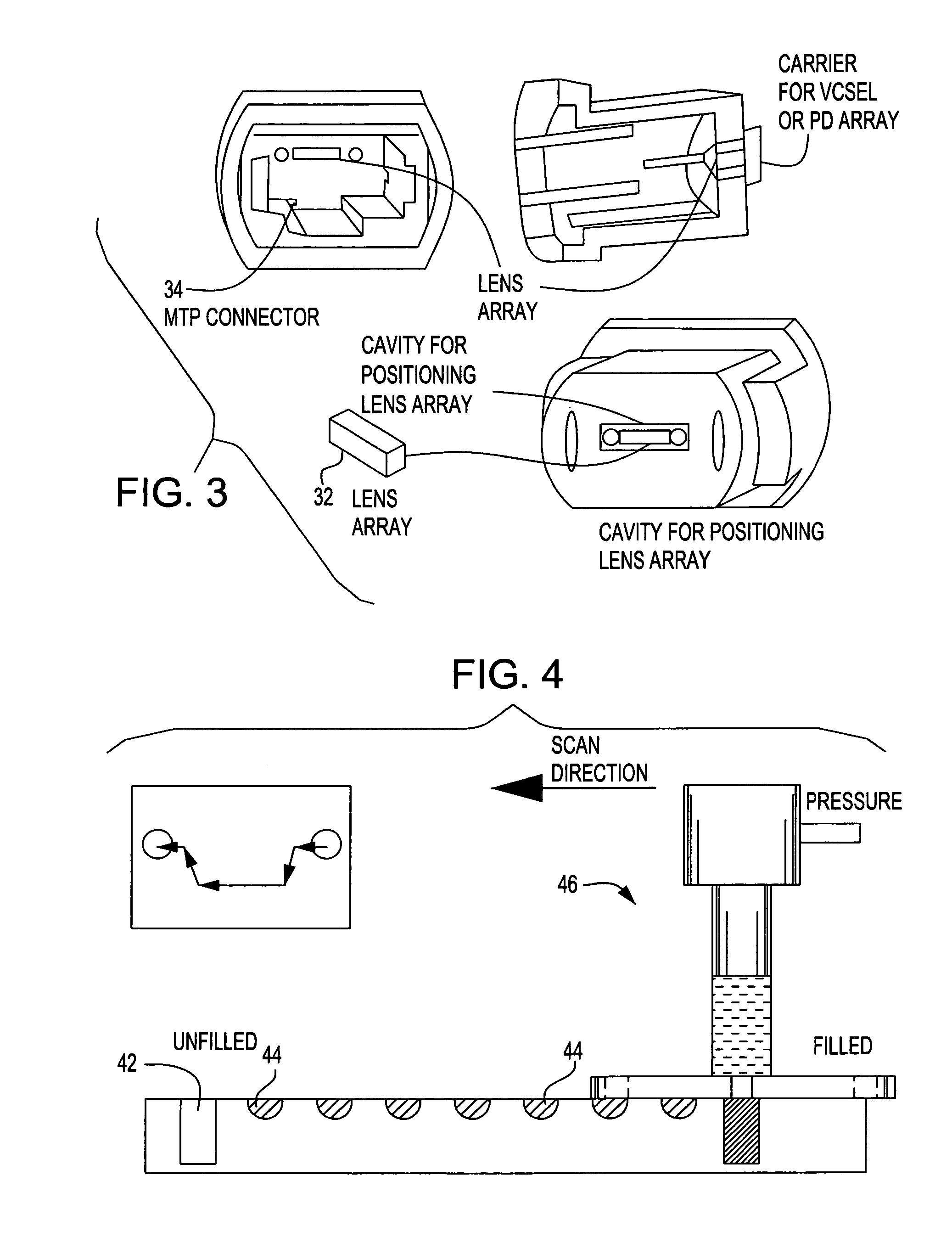
[0028]This invention relates to the fabrication of micro lenses, and more specifically, to micro lenses that are suited for use as optical connectors. As mentioned above, in order to achieve low cost, molded plastic optics has been used for fiber-to-detector coupling. Two basic types, thermoplastic and thermoset materials, have been employed in industry-standard multi-fiber push-on (MPO) connectors and in the multi-fiber termination (MT) ferrules which form the basis of these connector systems. As an alternative, glass materials are preferred since they are more stable over a wide temperature range and humidity environment than plastic. Additionally, glass materials provide more design freedom due to the availability of a wide variety of glasses with different types of doping, melting points, etc.

[0029]A preferred embodiment of the invention provides a glass micro lens array fabricated using wafer scale manufacturing approaches, because of its superior thermal performance and low ma...


PUM

PropertyMeasurementUnit
diameteraaaaaaaaaa
diameteraaaaaaaaaa
diameteraaaaaaaaaa

Abstract

Disclosed is a method of fabricating a molded structure including both micro lenses and metallic pins. The method comprises the steps of providing a mold apparatus having a set of first cavities and a set of second cavities, depositing a first material in the first cavities to form a set of metallic pins, and depositing a second material in the second cavities to form a set of micro lenses. The formed molded structure comprises a substrate, a set of molded microlenses on said substrate, and a set of molded metallic pins on that same substrate. The metallic pins may be formed as alignment pins or as electrical connectors. The invention enables the micro lenses and metallic pins to be manufactured by way of molding on a common substrate for the first time.

Description

CROSS-REFERENCE TO RELATED APPLICATIONS[0001]This application is related to the following co-pending applications, each of which is assigned to the same assignee as this application, International Business Machines Corporation of Armonk, N.Y. Each of the below listed applications is hereby incorporated herein by reference in its entirety:[0002]application Ser. No. 11 / 195,147, filed Aug. 2, 2005, for “Injection Molded MicroOptics,” and[0003]application Ser. No. 11 / 195,150, filed Aug. 2, 2005, for “Injection Molded Microlenses For Optical Interconnects, now U.S. Pat. No. 7,295,375.”BACKGROUND OF THE INVENTION[0004]1. Field of the Invention[0005]This invention generally relates to the fabrication of micro lens elements. More specifically, the invention relates to apparatus and methods for fabrication of micro lens elements and metal features, such as guide pins or electrical connectors, in a single molding process. The invention allows the optical micro lens and metallic connector elem...

Claims


Application Information

Patent Timeline
Patent Type & Authority Patents(United States)
IPC IPC(8): G02B27/10B29D11/00
CPCB29D11/00365C03B19/02
Inventor JACOBOWITZ, LAWRENCEDECUSATIS, CASIMER
Owner INT BUSINESS MASCH CORP
Why Eureka
Try Eureka