Contacts to semiconductor fin devices

Inactive Publication Date: 2006-09-12
TAIWAN SEMICON MFG CO LTD
View PDF4 Cites 88 Cited by
  • Summary
  • Abstract
  • Description
  • Claims
  • Application Information

AI Technical Summary

Benefits of technology

[0017]The method for forming a contact to a multiple-gate transistor may further include the step of providing a double-gate transistor, or the step of providing a triple-gate transistor, or the step of providing an omega field-effect transistor. The method may further include the step of forming the etch stop layer in a material that includes a dielectr

Problems solved by technology

Consequently, a transistor with a short gate length suffers from problems related to the inability of the gate to substantially control th on and off states of the channel.
However, for device scaling well into the sub-50 nm regime, the requirements for body-doping concentration, gate oxide thickness, and source/drain (S/D) doping profiles become increasingly difficult to meet when conventional device structures based on bulk silicon (Si) substrates are employed.
U.S. Pat. No. 6,413,802B1, however, does not teach the geometry en

Method used


Image

  • Contacts to semiconductor fin devices
  • Contacts to semiconductor fin devices
  • Contacts to semiconductor fin devices

Examples


Embodiment Construction

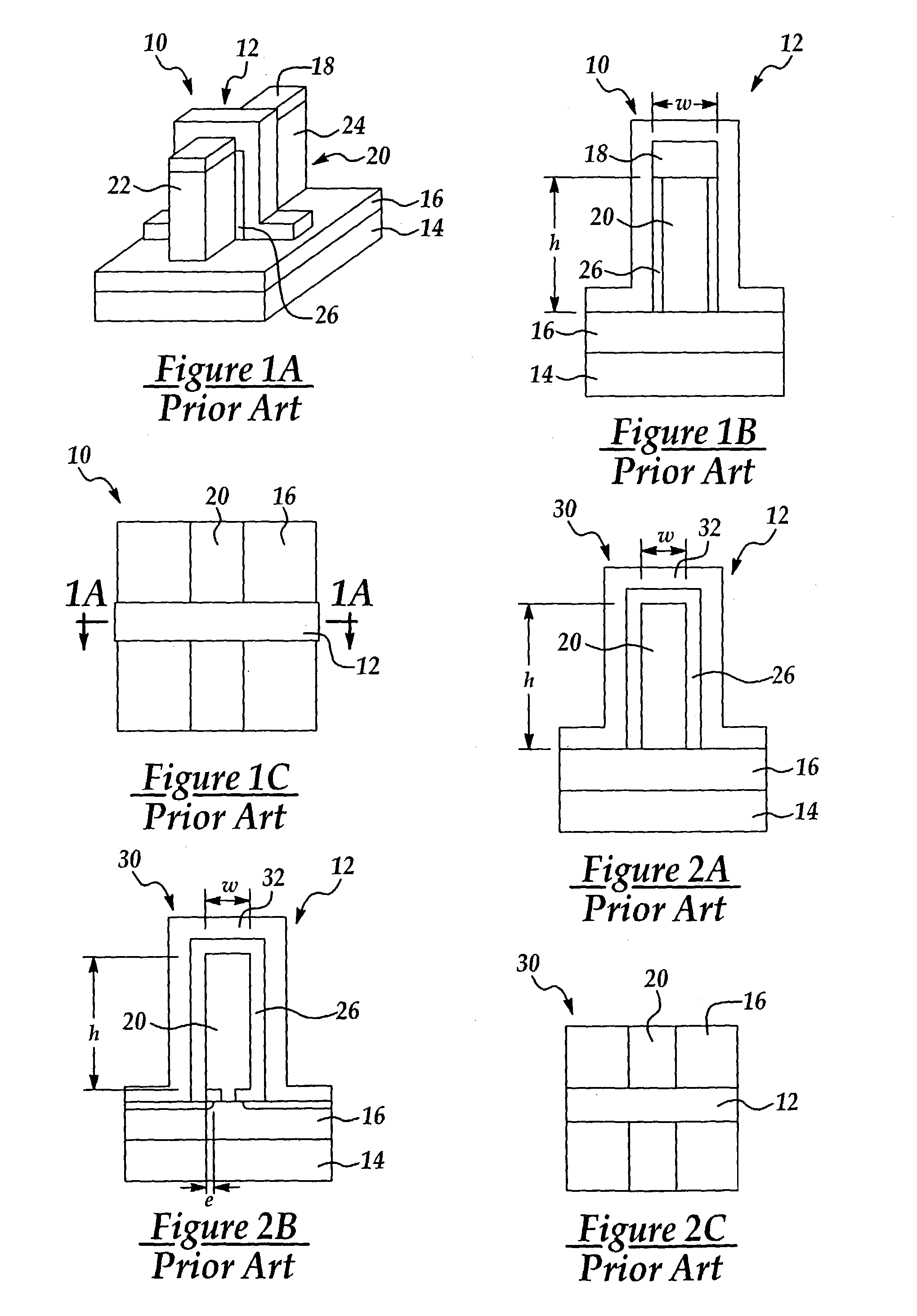
[0035]The present invention provides a method of forming a contact to the semiconductor fin with low contact resistance and large contact area.

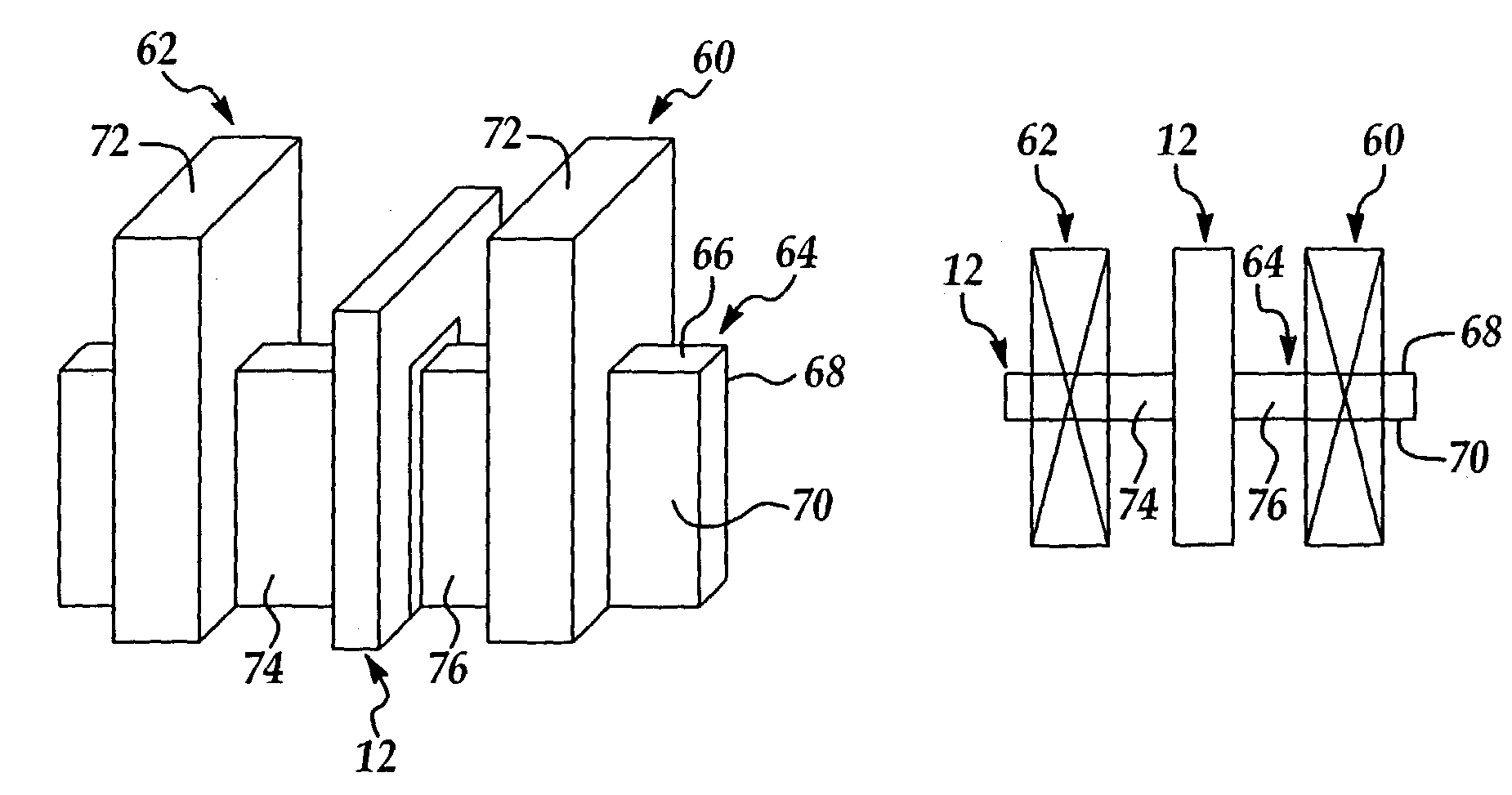
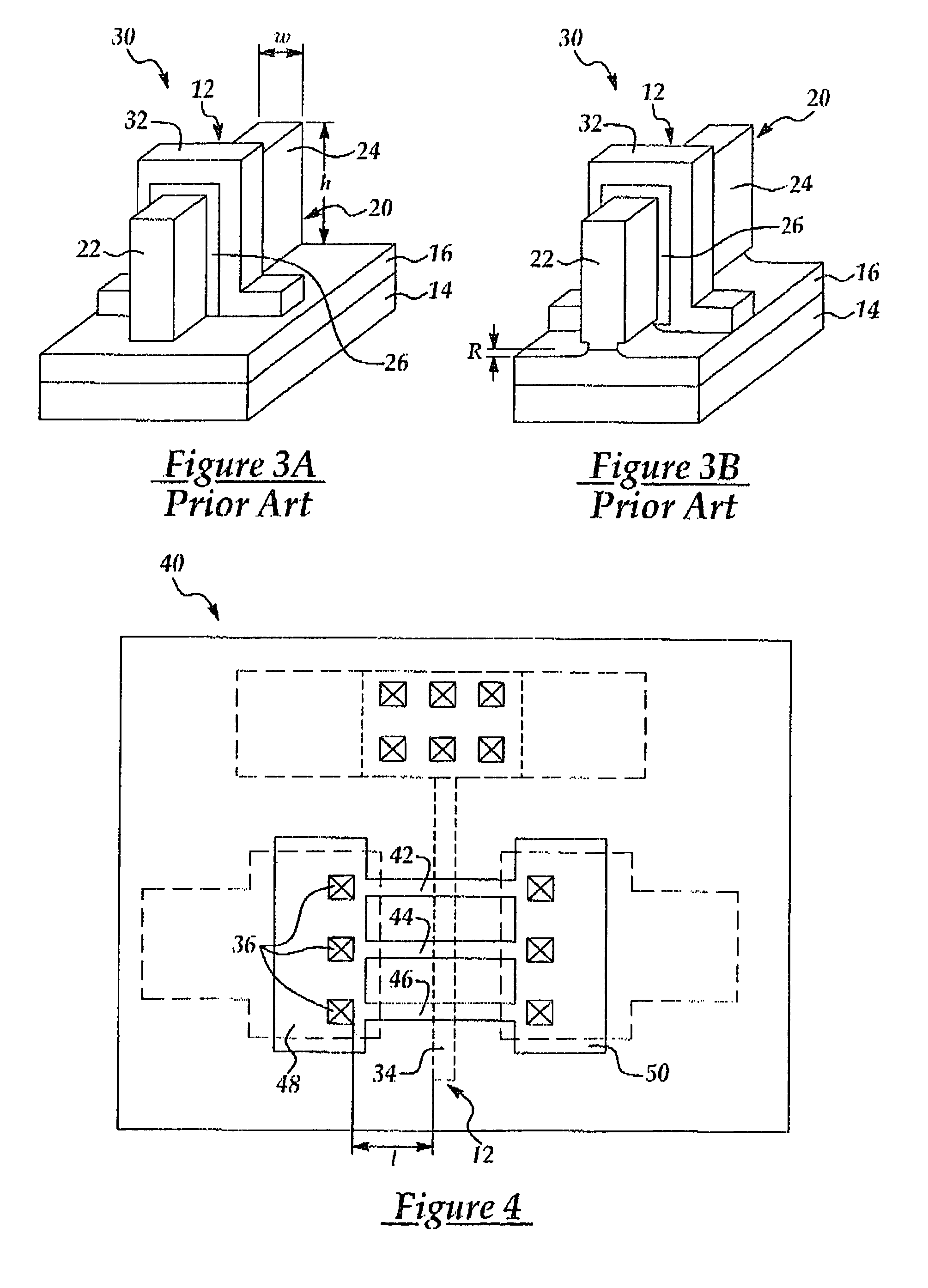
[0036]The conventional contact scheme may be improved since the contacts may be brought closer to the channel region for reduced series resistance. The series resistance is a function of the distance “1” between the contacts 36 and the transistor channel region 34, as shown in FIG. 4. A shorter distance leads to a lower series resistance. To shorten the distance between contacts and the channel region, contacts can be formed directly on the silicon fins. In act, if contact holes overlap the silicon fins and a contact hole formation process is modified to expose the silicon fins, it is possible that the conductive material makes contact with three surfaces of the fin, i.e. the top surface and the two sidewall surfaces.

[0037]In FIGS. 6A and 6B, a perspective view and a plane view of contacts 60,62 to a semiconductor fin 64 are illustrated, resp...


PUM


Abstract

A method for forming a contact to a semiconductor fin which can be carried out by first providing a semiconductor fin that has a top surface, two sidewall surfaces and at least one end surface; forming an etch stop layer overlying the fin; forming a passivation layer overlying the etch stop layer; forming a contact hole in the passivation layer exposing the etch stop layer; removing the etch stop layer in the contact hole; and filling the contact hole with an electrically conductive material.

Description

FIELD OF THE INVENTION[0001]The present invention relates to the field of semiconductor devices, and more specifically, to the manufacture of metal oxide semiconductor field effect transistors (MOSFETs) with multiple-gates and low contact resistances.BACKGROUND OF THE INVENTION[0002]The dominant semiconductor fabrication technology used for the manufacture of the ultra-large scale integrated (USLI) circuits is the metal-oxide-semiconductor field effect transistor (MOSFET) technology. Reduction in the size of MOSFETs has provided continued improvement in speed performance, circuit density, and cost per unit function over the past few decades. As the gate length of the conventional bulk MOSFET is reduced, the source and drain increasingly interact with the channel and gain influence on the channel potential. Consequently, a transistor with a short gate length suffers from problems related to the inability of the gate to substantially control th on and off states of the channel. Phenom...

Claims


Application Information

Patent Timeline
IPC IPC(8): H01L27/01H01L21/336H01L29/417H01L29/786
CPCH01L29/41791H01L29/66795H01L29/785H01L2029/7858H01L2924/0002H01L2924/00
Inventor YEO, YEE-CHIAYANG, FU-LIANGHU, CHENMING
Owner TAIWAN SEMICON MFG CO LTD
Why Eureka
Try Eureka