SiC semiconductor device and method for manufacturing the same

a semiconductor device and semiconductor technology, applied in the direction of semiconductor devices, basic electric elements, electrical appliances, etc., can solve the problem of insufficient channel mobility obtained in the method disclosed in patent document 4 and achieve the effect of increasing channel mobility

Inactive Publication Date: 2008-08-28
DENSO CORP
View PDF10 Cites 21 Cited by
  • Summary
  • Abstract
  • Description
  • Claims
  • Application Information

AI Technical Summary

Benefits of technology

[0015]Thus, at the time of the temperature reduction in the heat treatment step, the temperature is reduced to the termination-desorption temperature or less while continuously maintaining the wet atmosphere or hydrogen atmosphere in a temperature range of from 800 to 900° C., which is a termination-desorption temperature. This enables termination of the dangling bonds at the interface between the gate insulating film and the channel region with H or OH elements, thereby making it possible to obtain a silicon carbide semiconductor device having higher channel mobility.

Problems solved by technology

The channel mobility obtained in the method disclosed in Patent Document 4 is still insufficient and a further improvement in the channel mobility is expected.

Method used


Image

  • SiC semiconductor device and method for manufacturing the same
  • SiC semiconductor device and method for manufacturing the same
  • SiC semiconductor device and method for manufacturing the same

Examples


first embodiment

[0117]In view of the above examinations, a SiC semiconductor device is presented.

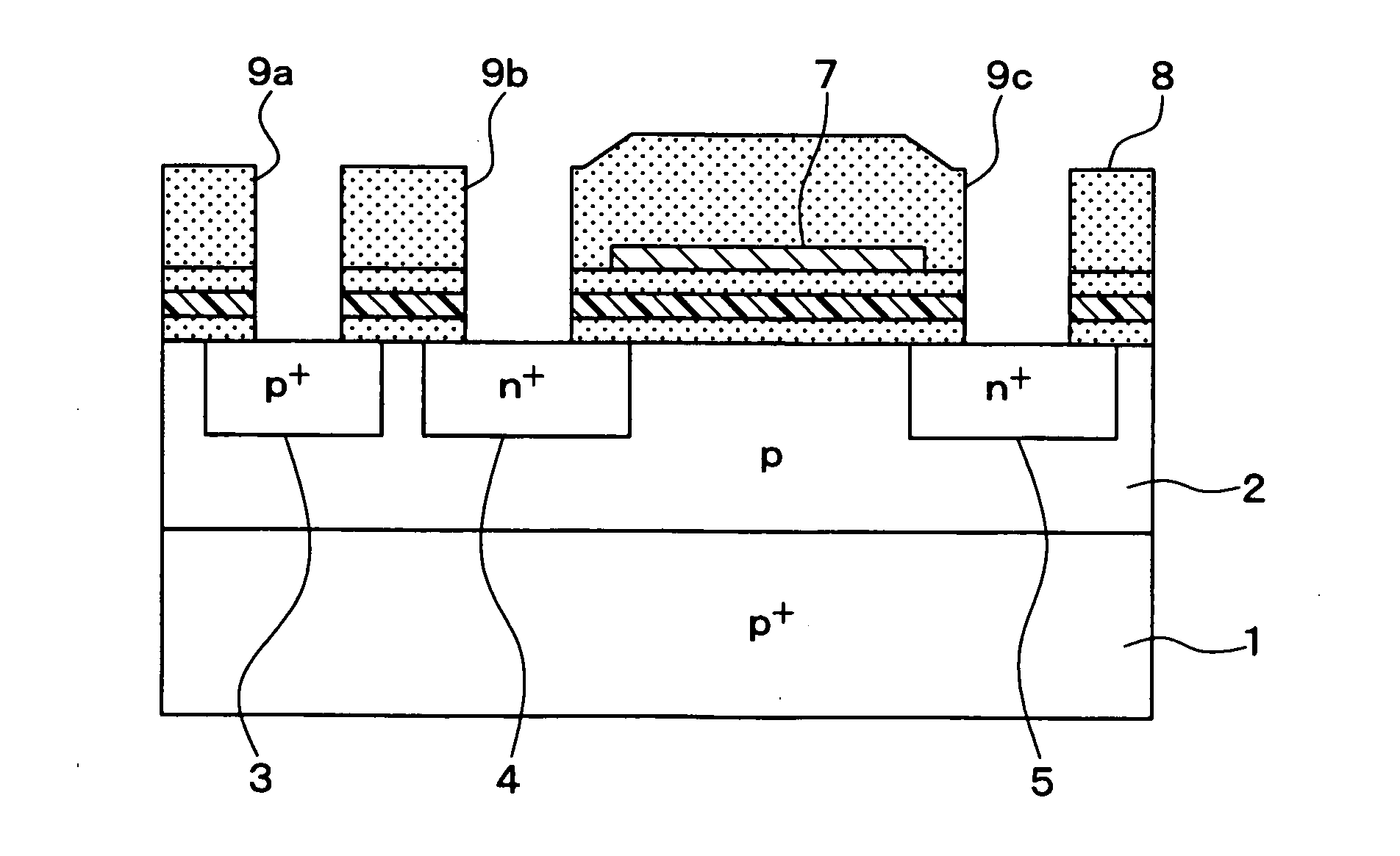
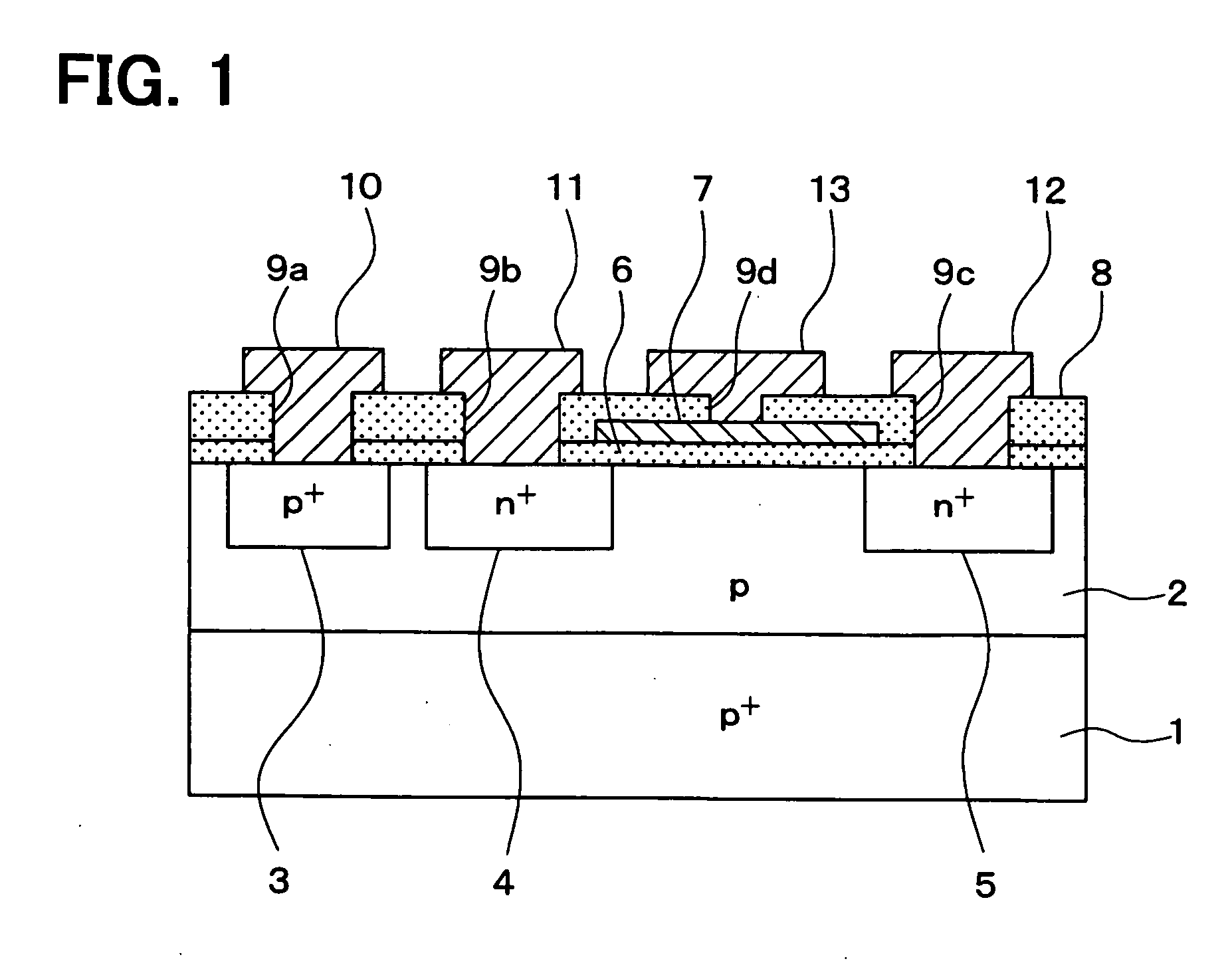
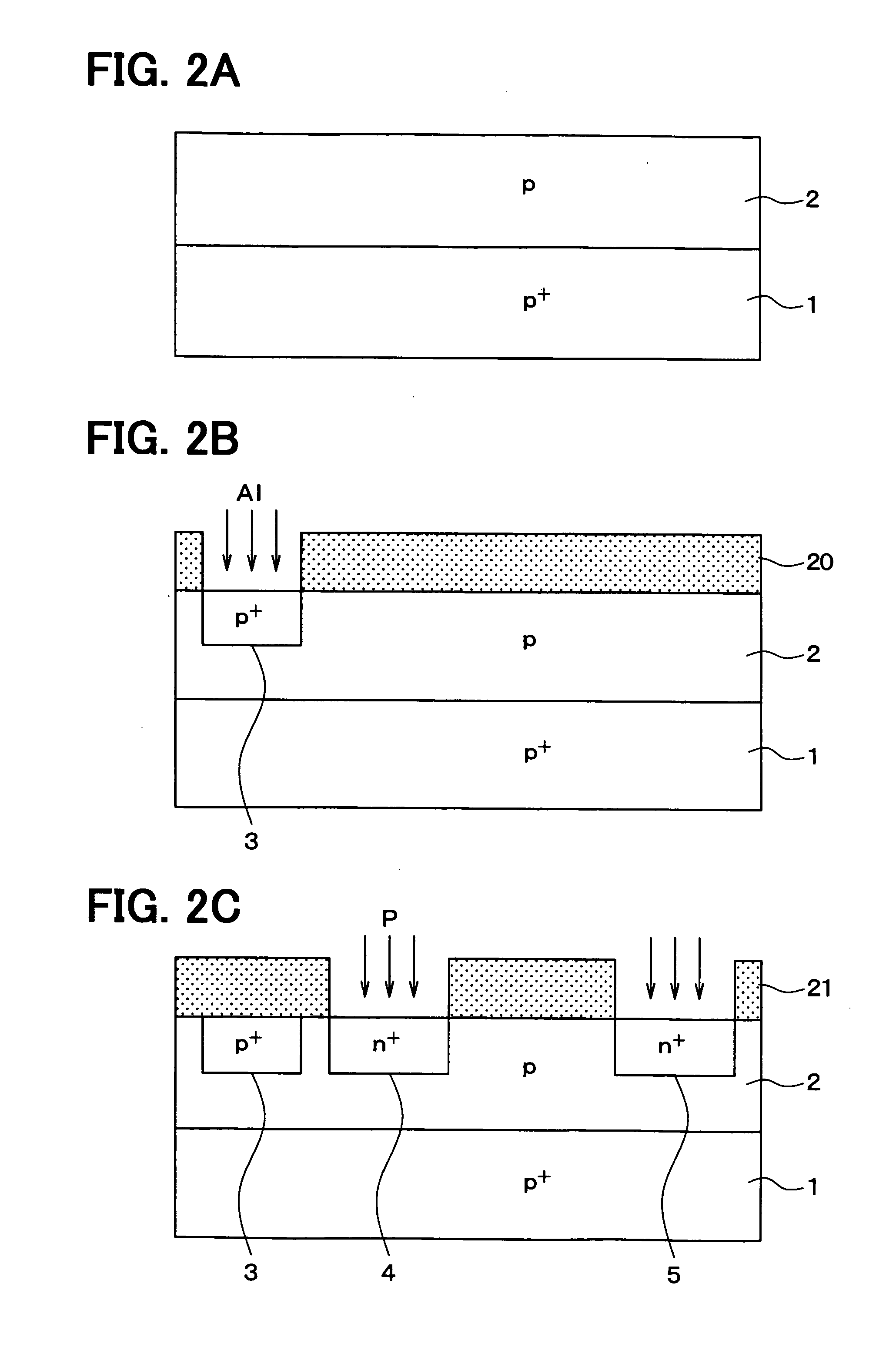
[0118]First embodiment of the present disclosure will be described. In this embodiment, one example is applied to an inversion mode lateral MOSFET. FIG. 1 illustrates a cross-sectional structure of the inversion mode lateral MOSFET, while FIGS. 2A to 3C illustrate manufacturing steps of the inversion mode lateral MOSFET of FIG. 1. With referent to these drawings, the structure and manufacturing method of the inversion mode lateral MOSFET according to this embodiment will be described.

[0119]As illustrated in FIG. 1, a p / p+ substrate obtained by forming, with one surface side of a p+ type substrate 1 made of SiC as a main surface, a p type base layer 2 made of epitaxially grown SiC on the main surface is used as a semiconductor substrate. The p+ type substrate 1 is, for example, a substrate which is made of 4H—SiC, has, as a main surface thereof, a (11-20) plane or a (1-100) plane, that is, a plane a vert...

second embodiment

[0140]Also in this embodiment, one example is applied to an inversion mode lateral MOSFET. The inversion mode lateral MOSFET according to the second embodiment has a similar structure to that according to the first embodiment but they differ partially in the manufacturing method. The inversion mode lateral MOSFET of this embodiment will next be described.

[0141]The inversion mode lateral MOSFET of this embodiment is manufactured by adding a manufacturing step shown in FIG. 6 to the manufacturing method of the inversion mode lateral MOSFET shown in FIGS. 2A to 3C in the first embodiment.

[0142]Described specifically, after respective steps shown in FIGS. 2A to 2C and FIGS. 3A and 3B, process shown in FIG. 6 is performed, followed by process shown in FIG. 3C and the like, whereby the inversion mode lateral MOSFET having a structure similar to that of the first embodiment is manufactured.

[0143]Described specifically, round-off oxidation of the surface of the gate 7 formed in the step sho...

third embodiment

[0149]In this embodiment, one example is also applied to an inversion mode lateral MOSFET. The inversion mode lateral MOSFET according to this embodiment has a similar structure to that of Embodiment 1 or 2, but they are partially different from each other in the manufacturing method. The inversion mode lateral MOSFET of this embodiment will next be described.

[0150]The inversion mode lateral MOSFET according to this embodiment is manufactured in a similar manner to that employed for the inversion mode lateral MOSFET shown in FIGS. 2A to 3C (and FIG. 6) except that the step of forming the interlayer insulating film 8 shown in FIG. 3C is changed to steps shown in FIGS. 8A and 8B.

[0151]Described specifically, after the respective steps shown in FIG. 2A to FIG. 2C and FIGS. 3A and 3B (or after the process shown in FIG. 6), processes shown in FIGS. 8A and 8B are performed instead of the process shown in FIG. 3C, whereby an inversion mode lateral MOSFET having a similar structure to that ...


PUM


Abstract

A SiC semiconductor device includes: a SiC substrate having a main surface; a channel region on the substrate; first and second impurity regions on upstream and downstream sides of the channel region, respectively; a gate on the channel region through a gate insulating film. The channel region for flowing current between the first and second impurity regions is controlled by a voltage applied to the gate. An interface between the channel region and the gate insulating film has a hydrogen concentration equal to or greater than 2.6×1020 cm−3. The interface provides a channel surface perpendicular to a (0001)-orientation plane.

Description

CROSS REFERENCE TO RELATED APPLICATION[0001]This application is based on Japanese Patent Application No. 2007-49703 filed on Feb. 28, 2007, the disclosure of which is incorporated herein by reference. This application is also related to U.S. application Ser. No. ______, entitled “SIC SEMICONDUCTOR DEVICE AND METHOD FOR MANUFACTURING THE SAME”, filed on ______.FIELD OF THE INVENTION[0002]The present invention relates to a SiC semiconductor device and a method for manufacturing a SiC semiconductor device.BACKGROUND OF THE INVENTION[0003]In Patent Documents 1 to 3, a forming method of an MOS interface is disclosed based on test results using a substrate having a (0001) Si plane. The channel mobility of an MOSFET having a channel formed on the (0001) Si plane thereof however does not become 10 cm2 / Vs or greater.[0004]In Patent Document 4, on the other hand, disclosed is a method of increasing the channel mobility in an MOS structure to 30 cm2 / Vs or greater by subjecting an SiC semicond...

Claims


Application Information

Patent Timeline
Patent Type & Authority Applications(United States)
IPC IPC(8): H01L29/15H01L21/3205H01L21/336
CPCH01L21/049H01L29/045H01L29/0847H01L29/7828H01L29/51H01L29/66068H01L29/1608H01L29/513H01L29/518H01L29/78
Inventor ENDO, TAKESHIYAMAMOTO, TSUYOSHIOKUNO, EIICHI
Owner DENSO CORP
Why Eureka
Try Eureka