Field-effect transistor, complementary field-effect transistor, and method of manufacturing field-effect transistor

a field-effect transistor and field-effect technology, applied in transistors, electrical devices, semiconductor devices, etc., can solve the problems of difficult to improve an on-state current as a channel width is reduced, and achieve the effect of reducing channel mobility, effective channel width, and increasing channel mobility securely

Inactive Publication Date: 2006-03-09
NEC ELECTRONICS CORP +1
View PDF4 Cites 23 Cited by
  • Summary
  • Abstract
  • Description
  • Claims
  • Application Information

AI Technical Summary

Benefits of technology

[0035] Channel mobility of a field-effect transistor (MOSFET) is known to be changed by the crystal plane orientation of Si (for example, T. Sato, Physical Review B, vol. 4, NO. 6, pp. 1950-1960 and 1971). Since the effective mass of a career (an electron or a hole) varies in the crystal plane orientation of Si, the channel mobility of MOSFET changes. The channel mobility of the hole (the career of the P channel field-effect transistor) is the smallest at the {001} plane, and it is increased with the inclination therefrom. Therefore, in the P channel field-effect transistor, according to the change of plane orientation of the inclined plane from <010> crystal axis direction to the <ab0> crystal axis direction (wherein “a” and “b” are independently an integer) or to a direction equivalent to the <ab0> crystal axis, the channel mobility can securely be increased.
[0036] On the other hand, the channel mobility of the electron (the career of the N channel field-effect transistor) is the greatest at the {001} plane, and it is reduced with the inclination therefrom. Therefore, in the N channel field-effect transistor, in contrary to the case of P channel field-effect transistor, according to the change of the plane orientation of the inclined plane from <010> crystal axis direction to the <ab0> crystal axis direction (wherein “a” and “b” are independently an integer) or to a direction equivalent to the <ab0> crystal axis, the channel mobility is reduced, while effective channel width is increased by the inclined plane, thus the deterioration of the ON-state current can be suppressed.
[0037] Also, independently of the channel mobility, the forming of the inclined plane increases the effective channel width, so the ON-state current property improves both in the P channel field-effect transistor and in the N channel field-effect transistor. FIGS. 12 to 14 show the calculation result about the relation between an inclination angle θ of the inclined plane and the ON-state current.
[0038] In the P channel field-effect transistor, as shown in FIGS. 12A, 13A and 14A, the more the inclination angle θ is, that is, the more the plane orientation of the inclined plane is sloped from the {001} plane towards the {011} plane, the more the mobility is. Therefore, the ON-state current of the P channel field-effect transistor is increased by the double effects, one is the effect of the increase of the channel mobility given by the inclined plane, and another is the effect of the increase of the channel width.
[0039] On the other hand, in the N channel field-effect transistor, as shown in FIGS. 12B, 13B and 14B, the more the inclination angle θ is, that is, the more the plane orientation of the inclined plane is sloped from the {001} plane towards the {011} plane, the less the mobility is. Therefore, the ON-state current of the N channel field-effect transistor depends on the trade-off between the effect of the decrease of the channel mobility given by the inclined plane and the effect of the increase of the channel width.

Problems solved by technology

We have considered that since an ON-state current per a unit channel width is constant, that is, unchanged, it is difficult to improve an ON-state current as a channel width is reduced.

Method used


Image

  • Field-effect transistor, complementary field-effect transistor, and method of manufacturing field-effect transistor
  • Field-effect transistor, complementary field-effect transistor, and method of manufacturing field-effect transistor
  • Field-effect transistor, complementary field-effect transistor, and method of manufacturing field-effect transistor

Examples


embodiment 1

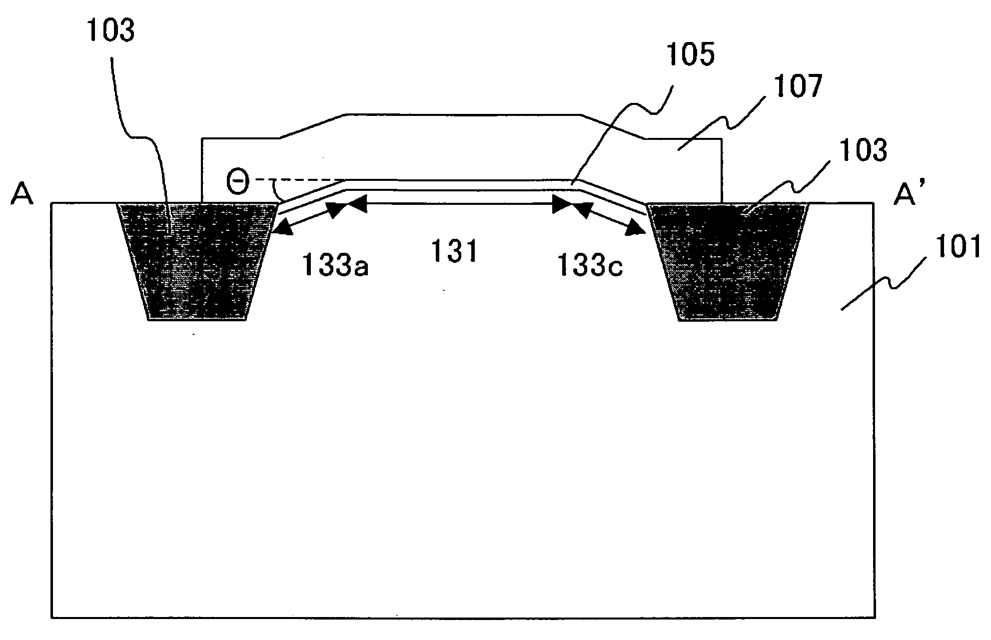
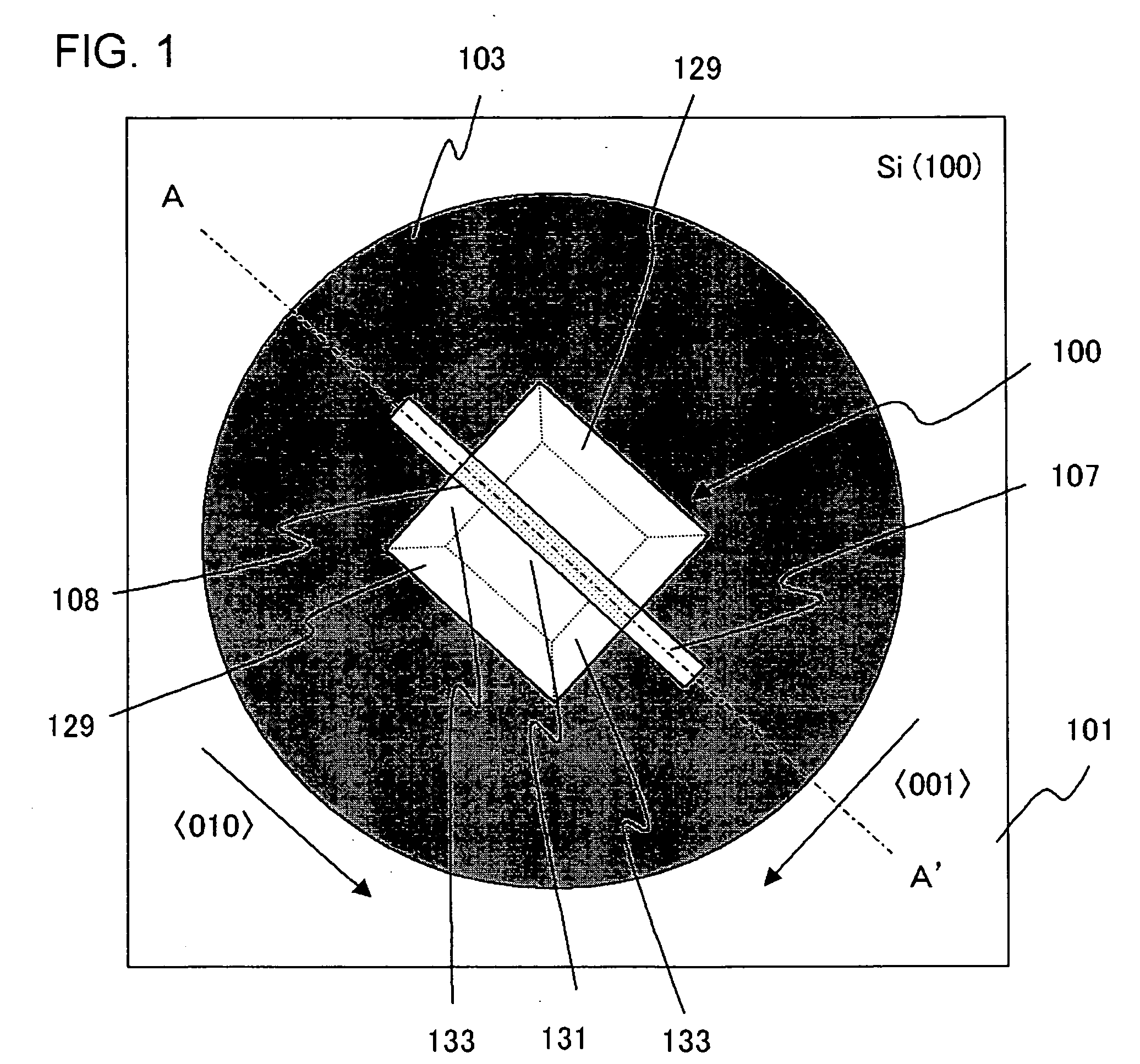
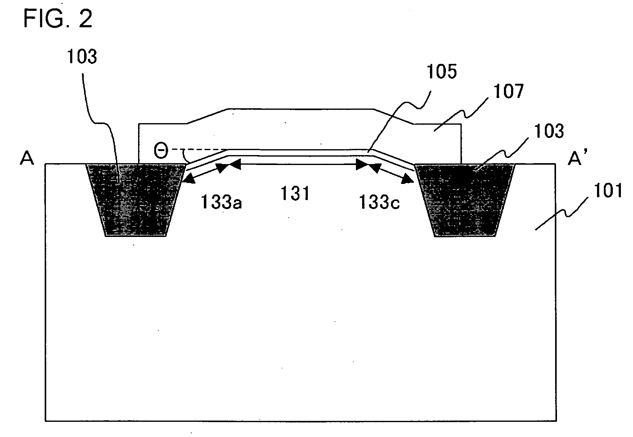
[0058] This embodiment relates to a P channel type MOSFET. FIG. 1 is a plan view showing a configuration of an MOS type transistor (P channel type MOSFET) according to this embodiment. FIG. 2 is a cross-sectional view taken on line A-A′ of FIG. 1. FIG. 3 is a perspective view schematically showing a configuration near a gate electrode 107 in an MOS field-effect transistor 100.

[0059] The MOS field-effect transistor 100 shown in FIGS. 1 and 2 is formed on a single-crystal silicon substrate 101 having a {100} plane as a principal surface. This invention will be described in connection to an exemplary transistor where the principal surface in the single-crystal silicon substrate 101 is a (100) plane.

[0060] There is formed an element isolation region 103 surrounding the lateral sides of the MOS field-effect transistor 100. The element isolation region 103 is buried in the single-crystal silicon substrate 101. In a plan view, an element forming region surrounded by the element isolation...

embodiment 2

[0090] This embodiment relates to the MOS field-effect transistor 100 described in Embodiment 1 where the inclined surface 133 is curved.

[0091]FIG. 7 is a cross-sectional view schematically showing a configuration of a semiconductor device according to this embodiment, from the same direction as FIG. 2. In FIG. 7, both inclined surfaces 133a and 133c are curved.

[0092] Since in this configuration, the channel region 108 also has the inclined surface 133 as described in Embodiment 1, a relative area of the inclined surface 133 can be increased to an area of a region separating the source / drain regions 129 in the single-crystal silicon substrate 101 seen from the normal line of the principal surface. The inclined surfaces 133a to 133d are configured such that in the crystal axis direction of the single-crystal silicon or an axis direction equivalent to the crystal axis direction, the surface orientation of the inclined surface 133 varies from the crystal axis direction of the sing...

embodiment 3

[0095] This embodiment relates to the MOS field-effect transistor 100 as described in Embodiment 1, where all of the inclined surfaces 133a to 133d are constituted by a plurality of planes.

[0096]FIG. 8 is a cross-sectional view schematically showing a configuration of a semiconductor device according to this embodiment, from the same direction as FIG. 2. In FIG. 8, there is shown a configuration where all of the inclined surfaces 133a to 133c are constituted by three planes having a different surface orientation.

[0097] By this configuration, a plane having a given inclination angle θ can be formed in the inclined surface 133 as is in Embodiment 1, resulting in increase of a ratio of a region for forming the inclined surface 133 to a width of a region for forming the channel region 108 and improvement of channel mobility. Furthermore, since all of the inclined surfaces 133a to 133d are constituted by the plurality of planes, electric field concentration in the end of the element is...


PUM


Abstract

An objective of this invention is to improve an ON-state current of a field-effect transistor.
For this purpose, on a single-crystal silicon substrate 101 having a {100} plane as a principal surface are formed a gate electrode 107 extending substantially in a <010> crystal axis direction of the single-crystal silicon or an axis direction equivalent to the <010> crystal axis direction, and in both sides of the gate electrode 107, source/drain regions 129 on the surface of the single-crystal silicon substrate 101. On the surface of the single-crystal silicon substrate 101 in a region directly below the gate electrode 107 are formed a principal surface and an inclined surface 133 oblique to the principal surface along the extension direction of the gate electrode 107.

Description

[0001] This application is based on Japanese patent application NO. 2004-240752, the content of which is incorporated hereinto by reference. BACKGROUND OF THE INVENTION [0002] 1. Field of the Invention [0003] This invention relates to a field-effect transistor, a complementary field-effect transistor, and a method of manufacturing the field-effect transistor. [0004] 2. Description of the Related Art [0005] As the prior art, Japanese Patent Laid-open No. 2004-87640 has disclosed a technique for improving an operation speed of a transistor formed on a single-crystal silicon substrate having a (100) crystal plane as a principal surface. The publication has described that a channel direction of a field-effect transistor can be a <100> axis direction of silicon, allowing the transistor to be operated at a higher speed than that with a conventional <110> axis direction. It has also described that a stress controlling film can be formed on a field-effect transistor to improve d...

Claims


Application Information

Patent Timeline
Patent Type & Authority Applications(United States)
IPC IPC(8): H01L29/76H01L29/745
CPCH01L21/823807H01L21/823828H01L29/1037H01L27/092H01L29/045H01L21/823878
Inventor KASAI, NAOKINAKAHARA, YASUSHIKIMURA, HIROSHIFUKAI, TOSHINORI
Owner NEC ELECTRONICS CORP
Why Eureka
Try Eureka