Methods of thin film process

a thin film and process technology, applied in the direction of semiconductor devices, electrical apparatus, transistors, etc., can solve the problems of increasing the chances of electrical interference, difficult to fill spaces using conventional cvd methods, and the limitation of sputtering is an angular redistribution of sputtered material

Inactive Publication Date: 2008-07-31
APPLIED MATERIALS INC
View PDF99 Cites 273 Cited by
  • Summary
  • Abstract
  • Description
  • Claims
  • Application Information

AI Technical Summary

Benefits of technology

[0027]Accordingly to exemplary embodiments, the steps in the above-described method may be repeated for one or more additional cycles of etching and depositing dielectric layers. For example, a portion of the second dielectric layer deposited at the end of the above-described method may further interact with the reactant to form a second solid product that is sublimated in a thermal treatment to remove that portion of the second dielectric layer. A third dielectric layer may be formed on the remaining (i.e., non-etched) portion of the second dielectric layer. Additional etching and dielectric deposition cycles may be performed until a final dielectric layer is deposited that substantially fills the remaining spaces (e.g., a dielectric cap layer).

Problems solved by technology

The smaller sizes, however, mean device elements have to work closer together which can increase the chances of electrical interference, including cross-talk and parasitic capacitance.
These spaces are difficult to fill using conventional CVD methods.
However, a limitation associated with sputtering is an angular redistribution of sputtered material.
For example, in an STI gapfill, the sputtered SiO2 can be sputtered from above the trench and deposit on the sides of the trench, causing excess buildup, and limiting the opening through which bottom-up gapfill is achieved.
If there is too much re-deposition, the trench can close off before the bottom is filled, leaving a buried void within the trench.

Method used


Image

  • Methods of thin film process
  • Methods of thin film process
  • Methods of thin film process

Examples


exemplary embodiment 1

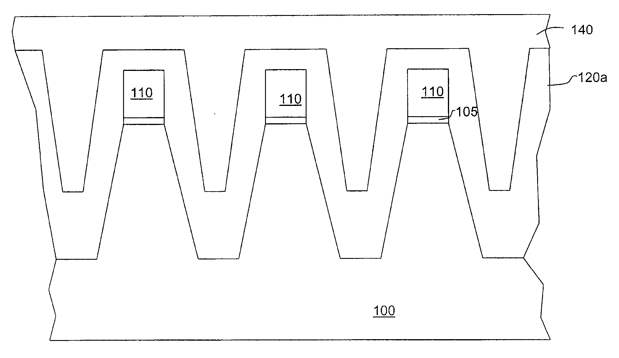
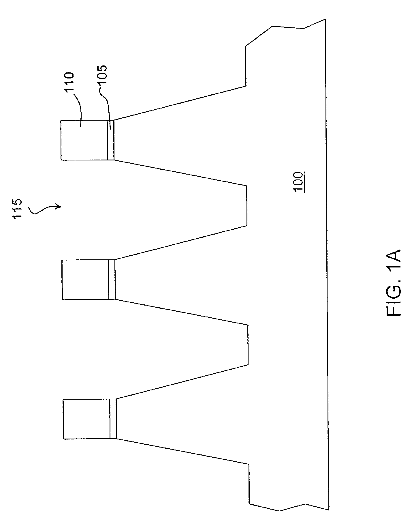
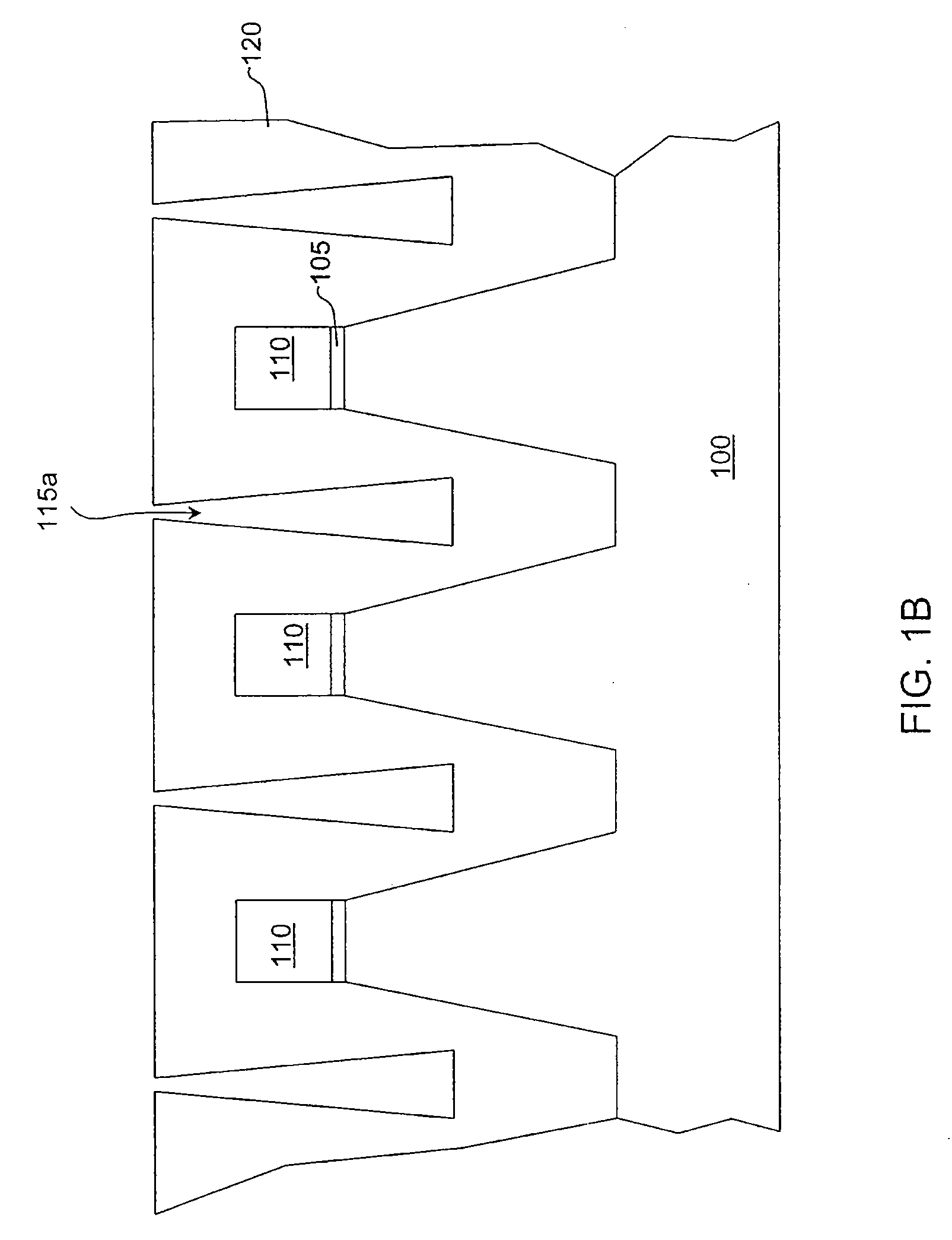
[0045]In some embodiments, the dielectric layer 120 can be a silicon oxide layer. A first precursor can be, for example, hydrogen (H2), ammonia (NH3), hydrazine (N2H4), hydrazoic acid (HN3), other hydrogen-containing precursor and various combinations thereof A second precursor can be, for example, nitrogen trifluoride (NF3), silicon tetrafluorid (SiF4), tetrafluoromethane (CF4), fluoromethane (CH3F), difluoromethane (CH2F2), trifluoromethane (CHF3), octafluoropropane (C3F8), hexafluoroethane (C2F6), other fluorine-containing precursor or various combinations thereof. In some embodiments, the first precursor such as ammonia (NH3) and the second precursor such as nitrogen trifluoride (NF3) can be ionized as a plasma. In some embodiments, the ionization process can be performed within the chamber that deposits the dielectric layer 120. In some embodiments, the ionization process can be occurred externally and then introduced into the chamber that deposits the dielectric layer 120. In ...

exemplary embodiment 2

[0050]In some embodiments, the dielectric layer 120 can be a silicon oxide layer. A first precursor can be, for example, hydrogen (H2), ammonia (NH3), hydrazine (N2H4), hydrazoic acid (HN3), other hydrogen-containing precursor and various combinations thereof A second precursor can be, for example, hydrogen fluoride (HF), nitrogen trifluoride (NF3), silicon tetrafluorid (SiF4), tetrafluoromethane (CF4), fluoromethane (CH3F), difluoromethane (CH2F2), trifluoromethane (CHF3), octafluoropropane (C3F8), hexafluoroethane (C2F6), other fluorine-containing precursor or various combinations thereof. In some embodiments, the first precursor such as ammonia (NH3) and the second precursor such as hydrogen fluoride (HF) can be used to interact with the dielectric layer 120. In some embodiments, NH3 and HF can be introduced within the chamber that deposits the dielectric layer 120. In some embodiments, NH3 and HF can be introduced within an etch chamber different from the deposition chamber so a...

exemplary embodiment 3

[0055]In some embodiments, the dielectric layer 120 can be a silicon nitride layer. A first precursor can be, for example, hydrogen (H2), ammonia (NH3), hydrazine (N2H4), hydrazoic acid (HN3), other hydrogen-containing precursor and various combinations thereof. A second precursor can be, for example, hydrogen fluoride (HF), nitrogen trifluoride (NF3), silicon tetrafluorid (SiF4), tetrafluoromethane (CF4), fluoromethane (CH3F), difluoromethane (CH2F2), trifluoromethane (CHF3), octafluoropropane (C3F8), hexafluoroethane (C2F6), other fluorine-containing precursor or various combinations thereof. A first precursor such as hydrogen (H2) and a second precursor such as nitrogen trifluoride (NF3) can be ionized as a plasma. In some embodiments, the ionization process can be occurred within the chamber that deposits the dielectric layer 120. In some embodiments, the ionization process can be occurred externally and then introduced into the chamber that deposits the dielectric layer 120. In...


PUM


Abstract

A method for forming a semiconductor structure includes forming a plurality of features across a surface of a substrate, with at least one space being between two adjacent features. A first dielectric layer is formed on the features and within the at least one space. A portion of the first dielectric layer interacts with a reactant derived from a first precursor and a second precursor to form a first solid product. The first solid product is decomposed to substantially remove the portion of the first dielectric layer. A second dielectric layer is formed to substantially fill the at least one space.

Description

CROSS-REFERENCES TO RELATED APPLICATIONS[0001]This application claims the benefit of U.S. Provisional Application No. 60 / 869,066, filed Dec. 7, 2006. This application is also related to the U.S. patent application filed on the same day as the present application having Attorney Docket No. A11598 / T76820, titled “Mult-step Dep-Etch-Dep High Aspect Ratio Process for Dielectric Gapfills.” The entire contents of both application are herein incorporated by reference for all purposes.[0002]This application is related to co-assigned U.S. Provisional Patent Application No. 60 / 803,499 to Lubomirsky et al, filed May 30, 2006, and titled “PROCESS CHAMBER FOR DIELECTRIC GAPFILL.” This application is related to co-assigned U.S. Pat. No. 6,387,207 to Janakiraman et al., issued May 14, 2002, and titled “INTEGRATION OF REMOTE PLASMA GENERATOR WITH SEMICONDUCTOR PROCESSING CHAMBER.” This application is related to and co-assigned U.S. Pat. No. 6,830,624 to Janakiraman et al., issued Dec. 14, 2004, and...

Claims


Application Information

Patent Timeline
Patent Type & Authority Applications(United States)
IPC IPC(8): H01L21/762
CPCH01L21/02164H01L21/0217H01L21/76232H01L21/31116H01L21/67253H01L21/3105H01L21/76H01L21/205
Inventor INGLE, NITIN K.TANG, JINGZHENG, YIYUAN, ZHENGGE, ZHENBINLU, XINLIANGKAO, CHIEN-TEHBANTHIA, VIKASHMCCLINTOCK, WILLIAM H.CHANG, MEI
Owner APPLIED MATERIALS INC
Why Eureka
Try Eureka