Three-dimensional semiconductor structure and method of manufacturing the same

a semiconductor and three-dimensional technology, applied in the direction of semiconductor devices, basic electric elements, electrical equipment, etc., can solve the problems of forming horizontal and vertical semiconductor devices on a single major surface of a substrate, consuming significant chip area, and lasers capable of driving the temperature of the semiconductor material to be greater than 800

Inactive Publication Date: 2010-07-29
BESANG
View PDF100 Cites 264 Cited by
  • Summary
  • Abstract
  • Description
  • Claims
  • Application Information

AI Technical Summary

Problems solved by technology

However, these laterally oriented devices consume significant amounts of chip area.
However, forming both horizontal and vertical semiconductor devices on a single major surface of a substrate complicates the processing steps because the required masks and processing steps are not compatible.
However, a disadvantage of this method is that the laser is capable of driving the temperature of the semiconductor material to be greater than 800 degrees Celsius (° C.).
In some situations,

Method used


Image

  • Three-dimensional semiconductor structure and method of manufacturing the same
  • Three-dimensional semiconductor structure and method of manufacturing the same
  • Three-dimensional semiconductor structure and method of manufacturing the same

Examples


Embodiment Construction

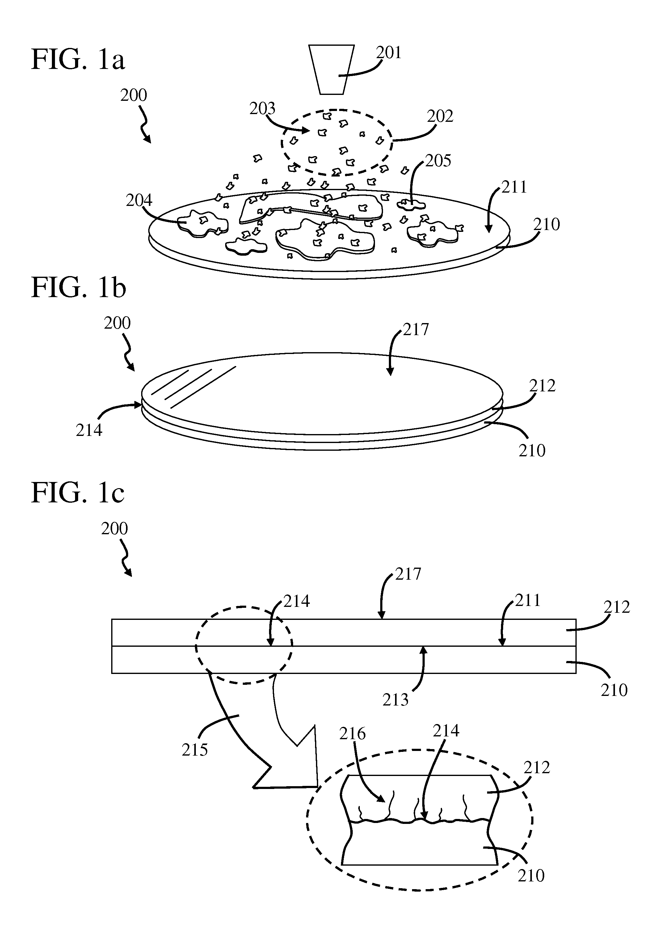
[0053]FIG. 1a is a perspective view of a partially fabricated grown semiconductor structure 200. In this embodiment, grown semiconductor structure 200 includes a substrate 210. Substrate 210 can be of many different types, such as a semiconductor substrate. A gaseous semiconductor material 203 is provided from a growth material source 201 in a region 202 proximate to a substrate surface 211 of substrate 210. It should be noted that, in general, more than one material sources are used to provide growth material and process gases. However, one material source is shown in FIG. 1a for simplicity and ease of discussion.

[0054]The semiconductor material discussed herein can be of many different types, such as silicon, germanium, silicon-germanium, gallium arsenide, gallium nitride, as well as alloys thereof. Further, substrate 210 can include a single layer structure, such as a silicon layer. However, in other embodiments, substrate 210 can include a multiple layer structure, such as a sil...


PUM


Abstract

A semiconductor circuit structure includes a support substrate which carries an interconnect region and electronic circuitry. The semiconductor circuit structure includes a device substrate coupled to the interconnect region through a conductive bonding layer. The device substrate includes a planarized surface which faces the conductive bonding layer. The device substrate can carry laterally oriented semiconductor devices which are connected to the electronic circuitry carried by the support substrate. The device substrate can be processed to form vertically oriented semiconductor devices which are connected, through the interconnect region and conductive bonding layer, to the electronic circuitry carried by the support substrate.

Description

CROSS-REFERENCE TO RELATED APPLICATIONS[0001]This patent application claims priority to Korean Patent Application No. 10-2009-24793, which was filed on Mar. 24, 2009 by the same inventor, the contents of which are incorporated by reference as though fully set forth herein.[0002]This application is a continuation-in-part of, and claims the benefit of, U.S. patent application Ser. Nos.:[0003]12 / 475,294, filed on Mar. 29, 2009;[0004]12 / 470,374, filed on Mar. 21, 2009;[0005]12 / 397,309, filed on Mar. 3, 2009;[0006]12 / 040,642, filed on Feb. 29, 2008,[0007]11 / 092,498, filed on Mar. 29, 2005,[0008]11 / 092,499, filed on Mar. 29, 2005,[0009]11 / 092,500, filed on Mar. 29, 2005,[0010]11 / 092,501, filed on Mar. 29, 2005;[0011]11 / 092,521, filed on Mar. 29, 2005;[0012]11 / 180,286, filed on Jul. 12, 2005;[0013]11 / 378,059, filed on Mar. 17, 2006; and[0014]11 / 606,523, filed on Nov. 30, 2006;which in turn are continuation-in-parts of, and claim the benefit of, U.S. patent application Ser. No. 10 / 873,969 (...

Claims


Application Information

Patent Timeline
IPC IPC(8): H01L21/768
CPCH01L21/2007H01L21/8221H01L2924/1305H01L2924/0132H01L2924/0665H01L2924/01033H01L2924/01023H01L2924/01006H01L2224/2919H01L24/29H01L2924/19043H01L2924/19042H01L2924/19041H01L2924/14H01L2924/13091H01L2924/07802H01L2924/04953H01L2924/04941H01L2924/01093H01L2924/01074H01L2924/01073H01L2924/0105H01L24/24H01L24/82H01L24/83H01L24/94H01L27/0688H01L2224/18H01L2224/291H01L2224/8385H01L2924/01005H01L2924/01013H01L2924/01015H01L2924/01029H01L2924/0104H01L2924/01042H01L2924/01049H01L2924/00H01L2924/01014H01L2924/01007H01L2924/01031H01L2924/01032H01L2924/3512H01L2924/12036
Inventor LEE, SANG-YUN
Owner BESANG
Why Eureka
Try Eureka