Solid State Light Emitting Device

a light-emitting device and solid-state technology, applied in the field of solid-state light-emitting devices and semiconductor devices, can solve the problems of inability to achieve the effect of green and longer wavelength light, weak indium-nitrogen bonding strength, and large amount of indium

Inactive Publication Date: 2009-06-25
PONCE FERNANDO A +2
View PDF9 Cites 280 Cited by
  • Summary
  • Abstract
  • Description
  • Claims
  • Application Information

AI Technical Summary

Problems solved by technology

However, the difficulty in growing device quality InGaN material with a large enough amount of indium (In) has inhibited the potential of these devices to emit green and longer wavelength light.
There are several problems associated with the growth of InGaN with a large amount of indium.
One problem is the weak strength of the indium-nitrogen (In—N) bond.
Ammonia (NH3) is generally used as the nitrogen source gas when growing nitride materials, but at low growth temperatures, it is more difficult to dissociate ammonia to provide nitrogen.
This makes it more difficult to incorporate nitrogen into the InGaN alloy.
Another problem is that there is a large lattice mismatch between InGaN and gallium nitride (GaN), which is another nitride material often included in InGaN-based devices.
However, the lattice mismatch between InGaN and GaN can be up to about 11%, which makes InGaN / GaN heterostructures highly strained.
Further, InGaN alloys are known to be thermodynamically unstable with these amounts of indium and, as a result, are known to undergo phase separation.
Hence, these attempts have provided InGaN films that are not device quality.
However, this design approach is difficult to utilize in mass production.
One reason for this is because of the difficulty in mounting the three separate LEDs in one package and providing external contacts to them.
For example, the mixing of blue and yellow light has little or no red component, so there is poor red color rendering capability.
Further, light conversion using this approach results in undesirable down conversion losses, which decreases the efficiency of the device.

Method used


Image

  • Solid State Light Emitting Device
  • Solid State Light Emitting Device
  • Solid State Light Emitting Device

Examples


Embodiment Construction

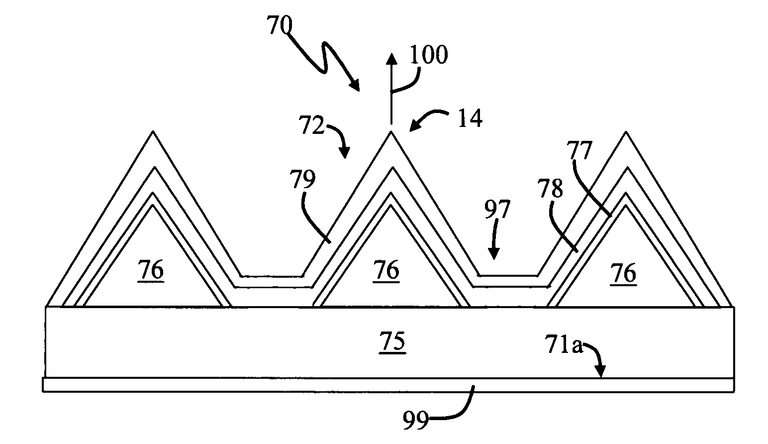
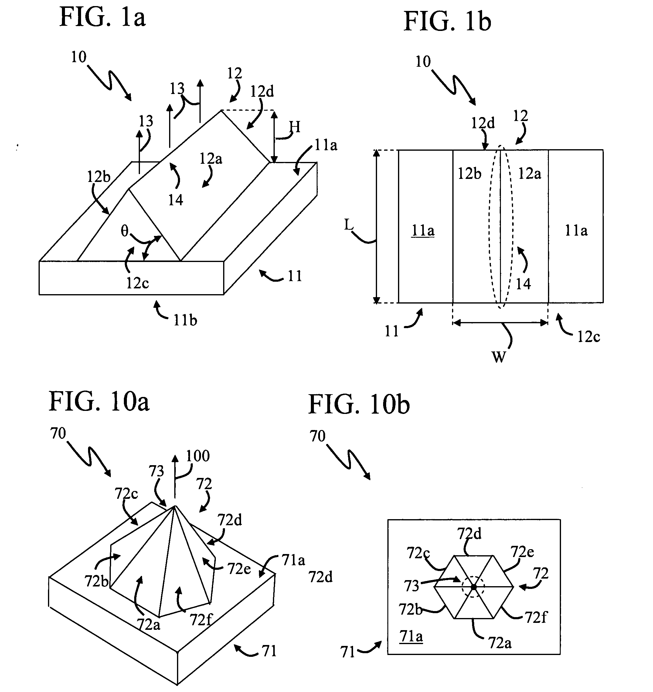
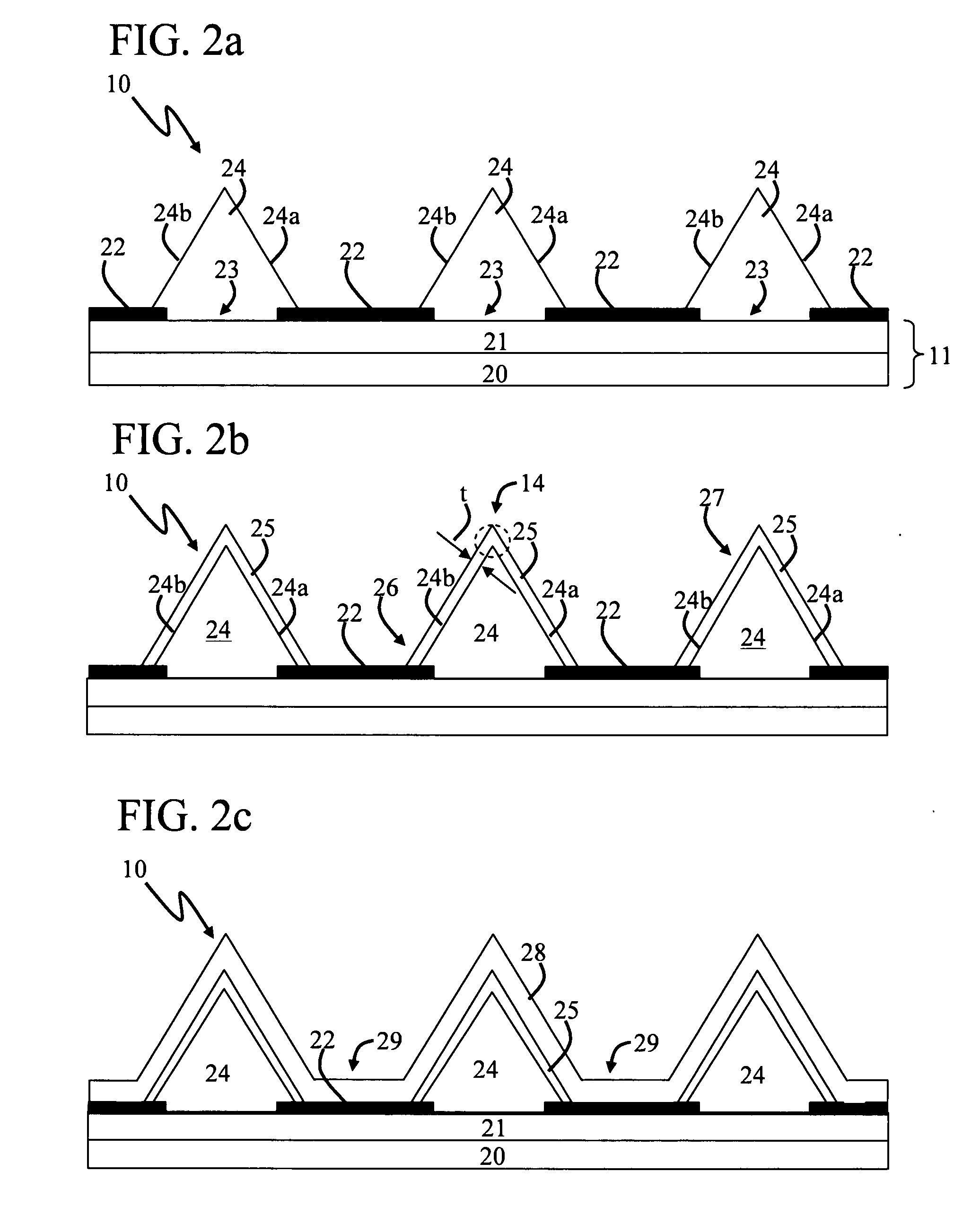
[0033]The invention includes several semiconductor structures that can operate as solid state light emitting devices and methods of operating and fabricating them. The semiconductor structures employ InGaN light emitting regions which are shaped so that there is a larger amount of indium in one portion of the light emitting region than others. The portion with the higher amount of indium is typically at or near an apex region of the light emitter. Because a larger amount of indium is incorporated in these regions, light of longer wavelength is emitted therefrom. These wavelengths include those in the green, yellow, and red spectrums, as well as the shades of light therebetween. Other portions of the light emitting region include less indium so they emit shorter wavelengths of light, such as those in the blue and violet spectrums, as well as the shades of light therebetween.

[0034]In some embodiments, the semiconductor structure can emit one or more wavelengths of light separately and...


PUM


Abstract

A semiconductor structure (10, 10′, 70, 80) includes a light emitter (12, 72) carried by a support structure (11). The light emitter (12, 72) includes a base region (24, 76) with a sloped sidewall (12a, 12b) and a light emitting region (25, 77) positioned thereon. The light emitting (25, 77) region includes a nitride semiconductor alloy having a composition that is different in a first region (26, 95) near the support structure (11) compared to a second region (27, 96) away from the support structure (11).

Description

CROSS-REFERENCE TO RELATED APPLICATIONS[0001]This application claims benefit to U.S. Provisional Applications Ser. Nos. 60 / 661,166 and 60 / 661,251, which were both filed on Mar. 11, 2005 and are incorporated herein by reference.BACKGROUND OF THE INVENTION[0002]1. Field of the Invention[0003]This invention relates generally to semiconductor devices and, more particularly, to semiconductor devices which emit light.[0004]2. Description of the Related Art[0005]Indium gallium nitride (InGaN) alloys are important nitride materials for applications in solid state light emitting devices, such as light emitting diodes (LEDs) and laser diodes (LDs). The bandgap of these alloys can be changed from less than 1 electron volt (eV) to 3.4 eV by varying their composition. Hence, light emitting devices that include InGaN alloys in their active regions can emit light in the visible, ultraviolet (UV), and infrared (IR) regions of the electromagnetic spectrum.[0006]Many of these InGaN-based devices have...

Claims


Application Information

Patent Timeline
Patent Type & Authority Applications(United States)
IPC IPC(8): H01L33/00H01L21/18H01L33/20H01L33/24H01L33/32
CPCH01L27/153H01L33/32H01L33/24H01L33/20
Inventor PONCE, FERNANDO A.SRINIVASAN, SRIDHAROMIYA, HIROMASA
Owner PONCE FERNANDO A
Why Eureka
Try Eureka