Strained-channel multiple-gate transistor

a strain-channel multiple-gate transistor and transistor technology, applied in the field of multi-gate transistors, can solve the problems of increasing the difficulty of meeting the requirements of body-doping concentration, gate oxide thickness, and the inability of the transistor to substantially increase the effect of the short channel, and the inability of the transistor to substantially increase the effect of the gate length

Inactive Publication Date: 2005-02-15
TAIWAN SEMICON MFG CO LTD
View PDF10 Cites 274 Cited by
  • Summary
  • Abstract
  • Description
  • Claims
  • Application Information

AI Technical Summary

Benefits of technology

The method for fabricating a multiple-gate semiconductor structure may further include the step of forming the semi-conducting layer in a material including silicon, or including silicon and germanium. The method may further include the step of forming the insulating layer in a material including silicon oxide. The fin forming step may further include a fin surface smoothing step, while the fin surface smoothing step may further include sub-steps of sacrificial oxidation in high temperature annealing in a hydrogen ambient. The method may further include the step of forming the gate dielectric layer in a material including silicon oxide, or in a material including silicon oxynitride. The method may further include the step of forming the gate dielectric layer using a high permittivity material such as La2O3, Al2O3, HfO2, HfON and ZrO2. The high permittivity material may have a relative permittivity of at least 5. The method may further include the step forming the gate dielectric layer to a thickness between 3 Å and 100 Å. The method may further include the step of forming a different thickness of the gate dielectric layer on the sidewall surfaces and on the top surface of the fin.
The method may further include the step of forming the gate dielectric layer to a smaller thi

Problems solved by technology

Consequently, a transistor with a short gate length suffers from problems related to the inability of the gate to substantially control the on/off states of the channel.
When the gate length is scaled down into the sub-50 nanometer (nm) regime, the requirements for body-doping concentration, gate oxide thickness, and source/drain (S/D) doping profiles to control short-channel effects become increasingly difficult to meet when conventional device structures based on bulk silicon (Si) substrates are employed.
However, there has been no

Method used


Image

  • Strained-channel multiple-gate transistor
  • Strained-channel multiple-gate transistor
  • Strained-channel multiple-gate transistor

Examples


Embodiment Construction

The present invention discloses a method of manufacturing for strained channel field effect transistors with multiple-gates capable of scaling down the complementary metal-oxide-semiconductor (CMOS) technology well into the sub-50 nanometer (NM) regime.

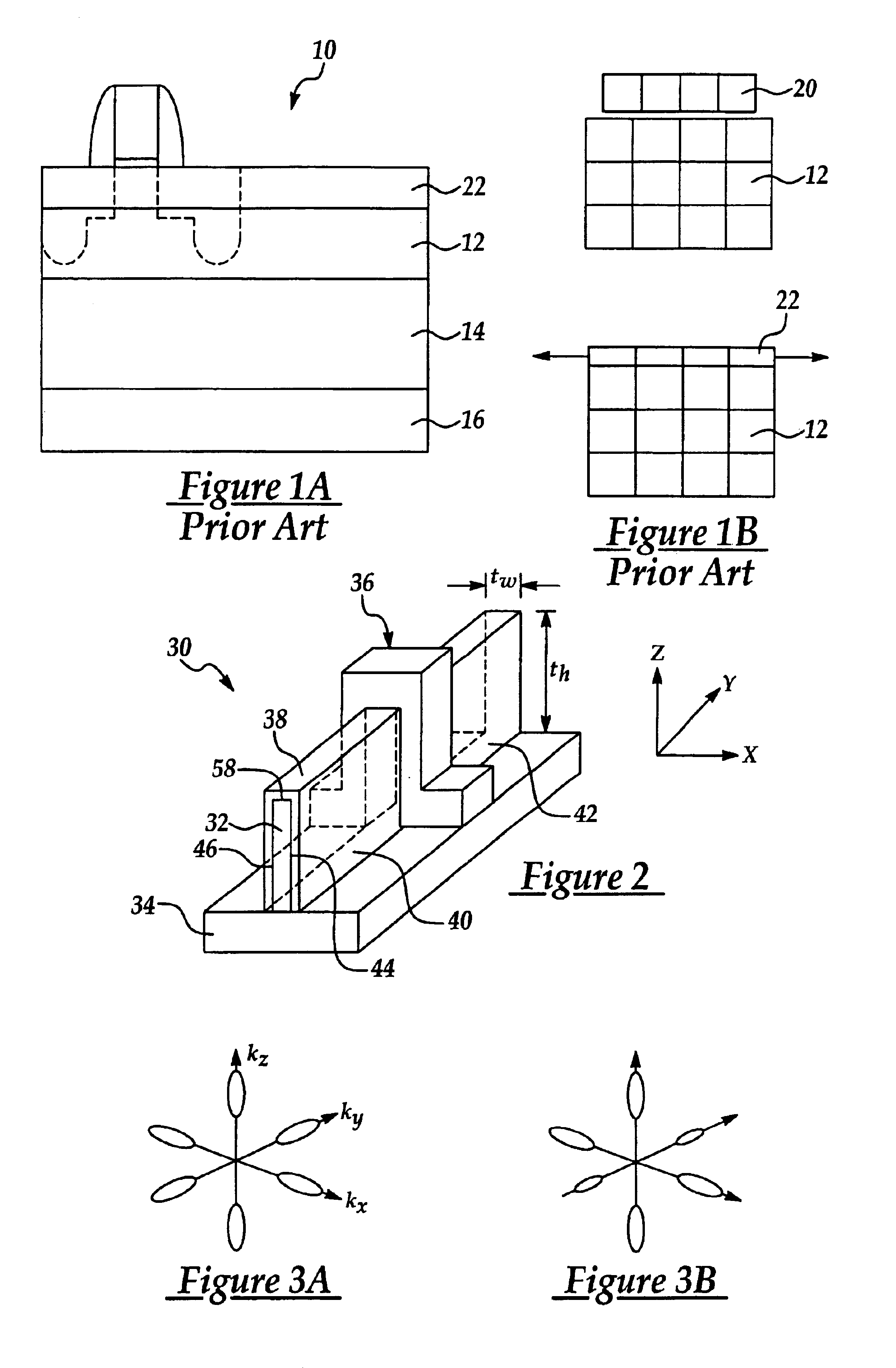
FIG. 1A illustrates a technique to induce strain in the Si channel of a conventional bulk MOSFET 10 by growing an epitaxial silicon (Si) layer 22 on a relaxed silicon-germanium (SiGe) layer overlying a silicon substrate 16. Relaxed SiGe layer 12 has a larger lattice constant compared to relaxed Si, and the thin layer 22 of epitaxial Si grown on the relaxed SiGe layer 12 will be under biaxial tensile strain, as shown in FIG. 1B. In the bulk MOSFET 10, both hole and electron mobilities are enhanced in the Si layer under biaxial tensile strain.

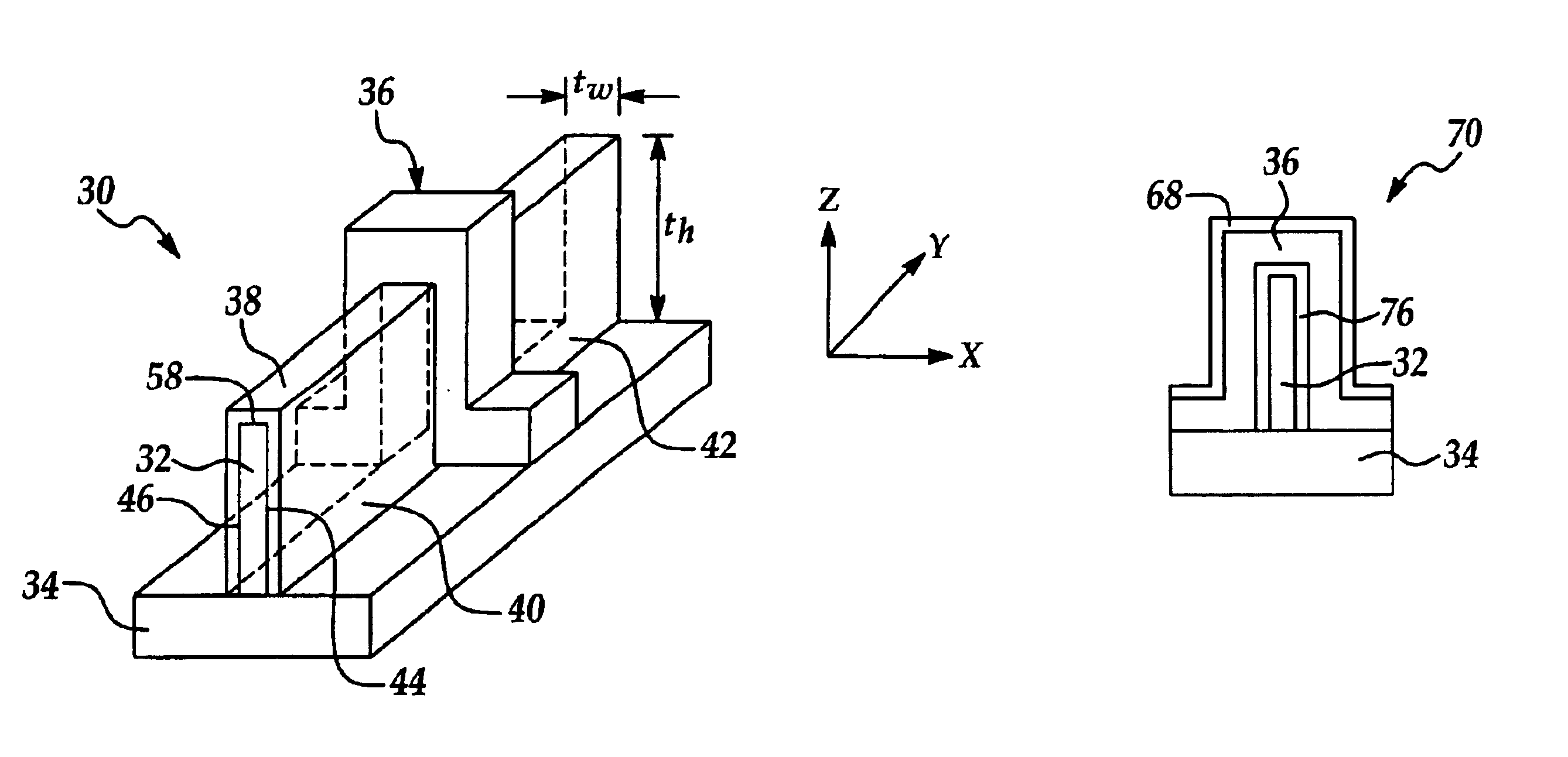
FIG. 2 illustrates a perspective view of a present invention multiple-gate transistor 30 formed with a fin-like channel 32. The fin-like channel 32 extend vertically from an insulating substrate 34...


PUM


Abstract

A multiple-gate semiconductor structure is disclosed which includes a substrate, a fin formed of a semi-conducting material that has a top surface and two sidewall surfaces. The fin is subjected to a strain of at least 0.01% and is positioned vertically on the substrate; source and drain regions formed in the semi-conducting material of the fin; a gate dielectric layer overlying the fin; and a gate electrode wrapping around the fin on the top surface and the two sidewall surfaces of the fin overlying the gate dielectric layer. A method for forming the multiple-gate semiconductor structure is further disclosed.

Description

FIELD OF THE INVENTIONThe present invention generally relates to a multiple-gate transistor and method for fabricating and more particularly, relates to a strained-channel multiple-gate transistor and method for fabrication.BACKGROUND OF THE INVENTIONSize reduction of the metal-oxide-semiconductor field-effect transistor (MOSFET) has enabled the continued improvement in speed performance, density, and cost per unit function of integrated circuits over the past few decades. As the gate length of the conventional bulk MOSFET is reduced, the interaction of the source and drain with the channel is increased resulting in gained influence on the channel potential. Consequently, a transistor with a short gate length suffers from problems related to the inability of the gate to substantially control the on / off states of the channel. Phenomena such as reduced gate control associated with transistors having short channel lengths are known as short-channel effects. Increased body doping concen...

Claims


Application Information

Patent Timeline
IPC IPC(8): H01L21/02H01L29/786H01L29/66H01L21/336H01L29/10H01L29/02
CPCH01L29/66795H01L29/78687H01L29/785H01L29/7842H01L29/1054H01L29/7854
Inventor YEO, YEE-CHIAYANG, FU-LIANGHU, CHENMING
Owner TAIWAN SEMICON MFG CO LTD
Why Eureka
Try Eureka