Multichip semiconductor device, chip therefor and method of formation thereof

a semiconductor device and chip technology, applied in semiconductor devices, semiconductor/solid-state device details, electrical apparatus, etc., can solve the problems of difficult electrical testing of each chip, limited number of chips that can be stacked, and multi-chip semiconductor devices, etc., to achieve small thickness, simple structure, and small plane area

Inactive Publication Date: 2005-01-20
TOSHIBA MEMORY CORP
View PDF36 Cites 99 Cited by
  • Summary
  • Abstract
  • Description
  • Claims
  • Application Information

AI Technical Summary

Benefits of technology

[0012] It is therefore an object of the present invention to provide a multichip semiconductor device which has a small plane area, a simple structure, and a small thickness.

Problems solved by technology

However, these conventional multichip semiconductor devices have the following problems.
However, the device of FIG. 2 has a problem that the number of chips that can be stacked is limited to two.
In addition, it is difficult to electrically test each chip.
However, its structure is complex, its thickness is great, and its manufacturing cost is high.

Method used


Image

  • Multichip semiconductor device, chip therefor and method of formation thereof
  • Multichip semiconductor device, chip therefor and method of formation thereof
  • Multichip semiconductor device, chip therefor and method of formation thereof

Examples


first embodiment

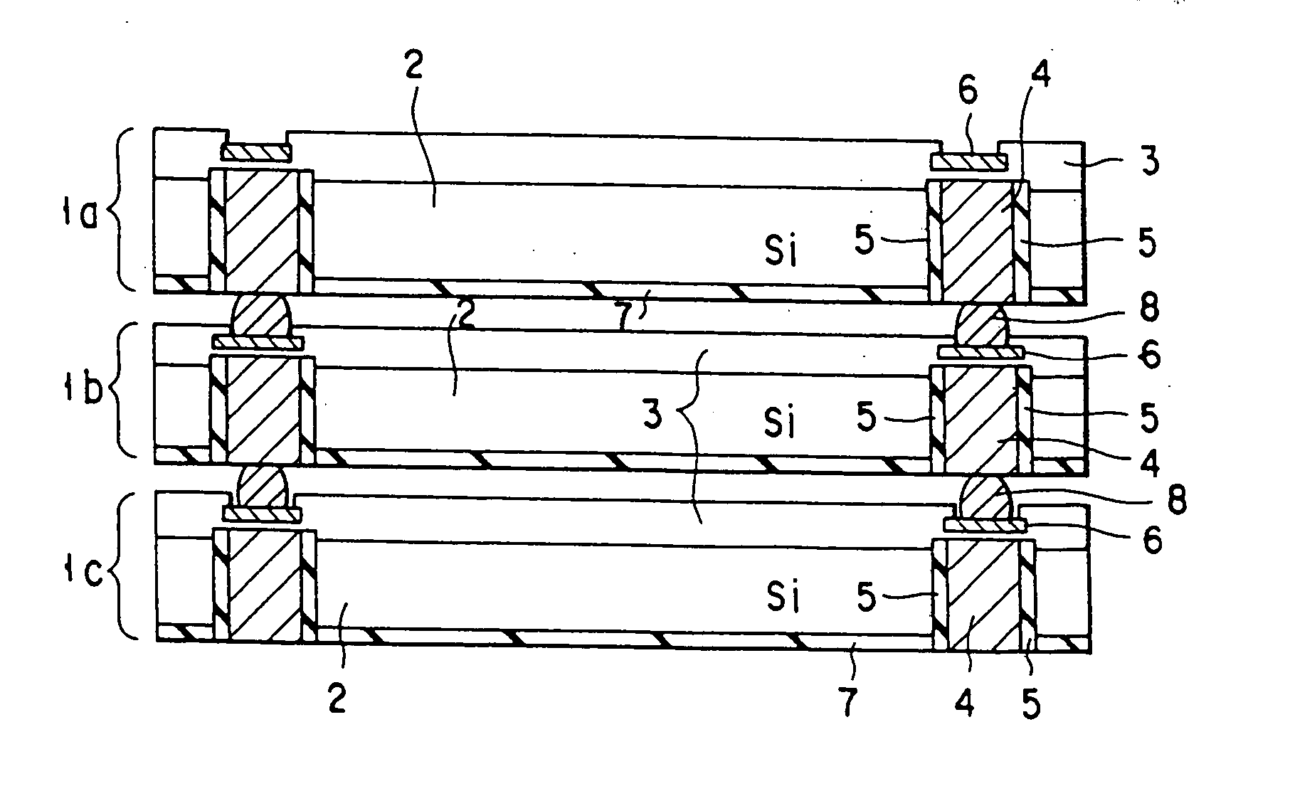
[0161] Referring now to FIG. 4, there is illustrated in section a multichip semiconductor device according to a first embodiment of the present invention.

[0162] This multichip semiconductor device is constructed such that three chips 1a, 1b and 1c are stacked. Each chip is constructed roughly from a silicon substrate 2 into which circuit devices or components are integrated, a multilevel interconnection layer 3 for interconnecting the circuit devices in a predetermined relationship, and connect plugs (each with a metal plug 4 and an insulating film 5) formed in through holes that are formed in the silicon substrate 2 and the first insulating film in the multilevel interconnection layer 3 and adapted to electrically connect it with another chip.

[0163] The multilevel interconnection layer 3 comprises a first interlayer insulating film that covers the circuit devices, a first interconnection layer that is connected with circuit devices through contact holes (first contact holes) form...

second embodiment

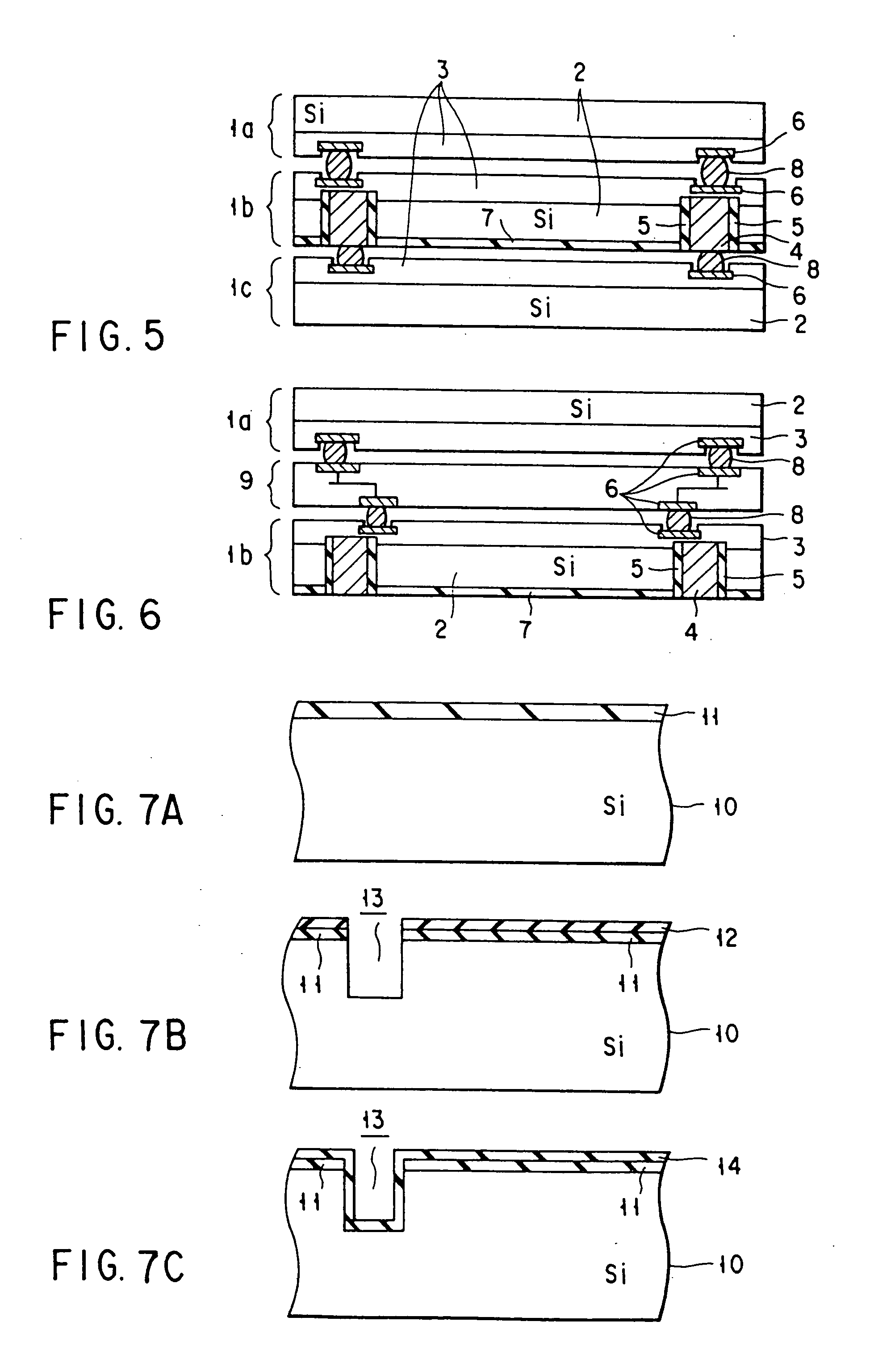
[0176]FIG. 5 is a sectional view of a multichip semiconductor device according to a second embodiment of the present invention. In this figure, like reference numerals are used to denote corresponding parts to those in FIG. 4 and their detailed descriptions are omitted.

[0177] This embodiment is designed such that only the center chip 1b has connect plugs (metal plug 4 and insulating film 5).

[0178] Pads 6 formed in the multilevel interconnection layer 3 of the chip 1a are electrically connected through solder bumps 8 with pads 6 formed in the multilevel interconnection layer 3 of the chip 1b, allowing the chips 1a and 1b to be electrically connected with each other.

[0179] Metal plugs 4 of the chip 1b are electrically connected through solder bumps 8 with pads 6 formed in the multilevel interconnection layer 3 of the chip 1c. In this manner, the chips 1a, 1b and 1c are electrically connected with one another.

[0180] The second embodiment provides the same advantages as the first em...

third embodiment

[0181]FIG. 6 is a sectional view of a multichip semiconductor device according to a third embodiment of the present invention. In this figure, like reference numerals are used to denote corresponding parts to those in FIG. 4 and their detailed descriptions are omitted.

[0182] In this embodiment, two chips 1a and 1b are connected together with an interconnecting substrate 9 made of a ceramic interposed therebetween.

[0183] The pads 6 formed in the multilevel interconnection layer 3 of the chip 1a are electrically connected through the solder bumps 8 with the pads 6 formed on the interconnecting substrate 9. The pads 6 formed on the rear side of the interconnecting substrate 9 each of which is electrically connected with a respective one of the pads on the top side of the substrate are electrically connected with the pads 6 formed in the multilevel interconnection layer 3 of the chip lb. Thus, the chips 1a and 1b are electrically connected with each other.

[0184] The third embodiment ...


PUM


Abstract

A multichip semiconductor device is disclosed in which chips are stacked each of which comprises a semiconductor substrate formed on top with circuit components and an interlayer insulating film formed on the top of the semiconductor substrate. At least one of the chips has a connect plug of a metal formed in a through hole that passes through the semiconductor substrate and the interlayer insulating film. The chip with the connect plug is electrically connected with another chip by that connect plug.

Description

CROSS-REFERENCE TO RELATED APPLICATIONS [0001] This is a Continuation-in-Part application of U.S. patent application Ser. No. 08 / 980,873, filed Dec. 1, 1997, the entire contents of which are incorporated herein by reference.BACKGROUND OF THE INVENTION [0002] The present invention relates to a multichip semiconductor device using multiple chips. [0003] The present invention also relates to a chip for a multichip semiconductor device and a method of manufacture thereof. [0004] Recent computers and communication equipment use for their important section a large-scale integrated circuit (chip) which has a great number of electronic components, such as transistors, resistors, etc., integrated into a semiconductor substrate. Thus, the performance of the entire equipment depends largely on the performance of the chip. [0005] On the other hand, so-called multichip semiconductor devices have proposed, each having a plurality of chips to improve the whole performance of the equipment. FIGS. 1...

Claims


Application Information

Patent Timeline
Patent Type & Authority Applications(United States)
IPC IPC(8): H01L21/768H01L23/48H01L23/64H01L25/065H01L25/10
CPCH01L21/76898H01L2224/14181H01L23/481H01L23/642H01L25/0657H01L25/105H01L25/50H01L2225/06513H01L2225/06527H01L2225/06541H01L2225/06572H01L2225/06589H01L2924/01046H01L2924/01057H01L2924/01078H01L2924/01079H01L2924/15174H01L2924/15192H01L2924/15311H01L2924/1532H01L2924/15331H01L25/0655H01L2224/16145H01L2224/16225H01L2224/32225H01L2224/73204H01L23/367H01L2924/13091H01L2924/10253H01L2225/1058H01L2225/1023H01L2924/00H01L2224/0401H01L2224/0557H01L2224/06181H01L2224/13025
Inventor HAYASAKA, NOBUOOKUMURA, KATSUYASASAKI, KEIICHIMATSUO, MIE
Owner TOSHIBA MEMORY CORP
Why Eureka
Try Eureka