Semiconductor device and method of manufacturing the same

a technology of semiconductor devices and semiconductors, applied in semiconductor devices, semiconductor/solid-state device details, electrical apparatus, etc., can solve the problems of low degree of freedom of wiring, large hole size, and large area required, and achieve the effect of increasing the degree of wiring freedom and enhancing functionality

Inactive Publication Date: 2005-08-25
SHINKO ELECTRIC IND CO LTD
View PDF8 Cites 237 Cited by
  • Summary
  • Abstract
  • Description
  • Claims
  • Application Information

AI Technical Summary

Benefits of technology

[0011] An object of the present invention is to provide a semiconductor device and a method of manufacturing the semiconductor device, in which when a semiconductor element (chip) is mounted in a package, miniaturization is realized and the degree of freedom of wiring is increased; in ...

Problems solved by technology

Consequently, the diameters of the through holes become relatively large (approximately 250 to 300 μm in the state of the art), and there has been the disadvantage in that a larger area is accordingly required.
Further, there are constraints on design (i.e., the degree of freedom of wiring is low), such as a technical difficu...

Method used


Image

  • Semiconductor device and method of manufacturing the same
  • Semiconductor device and method of manufacturing the same
  • Semiconductor device and method of manufacturing the same

Examples


first embodiment

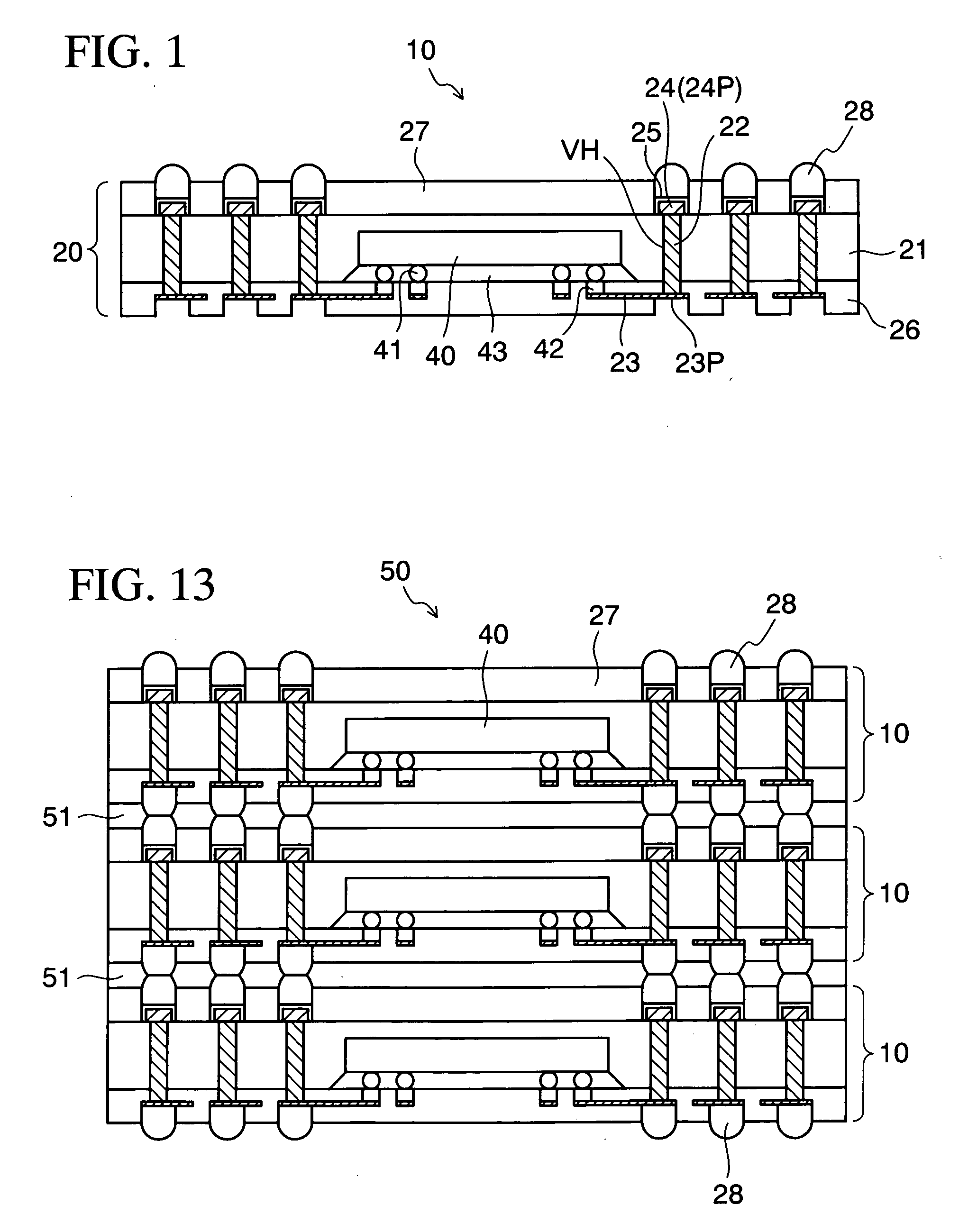
[0036]FIG. 1 schematically shows a cross-sectional structure of a semiconductor device according to the present invention.

[0037] The semiconductor device 10 according to this embodiment includes a wiring board 20 used as a package, and a semiconductor element (silicon (Si) chip) 40 buried in this package (wiring board) 20. In the illustrated example, one semiconductor chip 40 is buried in one package. However, two or more semiconductor chips 40 may be appropriately buried therein depending on functions required for the present device 10.

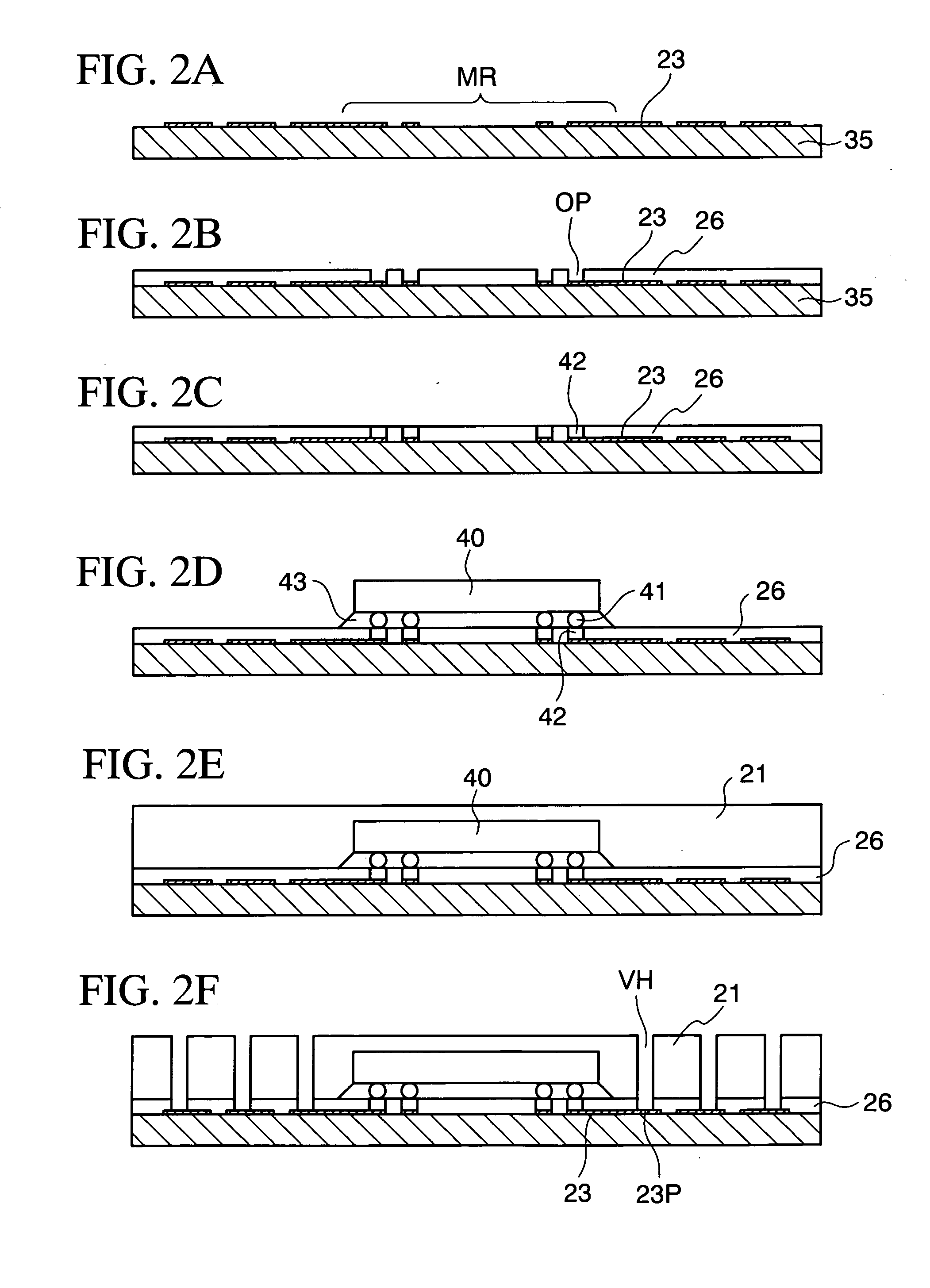
[0038] In the package (wiring board) 20, reference numeral 21 denotes an insulating base material (e.g., a resin layer made of epoxy resin or the like) which serves as a base for the wiring board. In this resin layer 21, via holes VH piercing the resin layer 21 in the thickness direction are formed in a region around the semiconductor chip 40. These via holes VH are filled with conductors 22 (e.g., metal such as copper (Cu)). One end (lower surface ...

second embodiment

[0061]FIG. 4 schematically shows a cross-sectional structure of a semiconductor device according to the present invention.

[0062] In this embodiment, similar to the first embodiment (FIG. 1), the semiconductor device 10a includes a wiring board 20a used as a package, and the semiconductor chip 40 buried in this package (wiring board) 20a. The package (wiring board) 20a in this embodiment differs from the package (wiring board) 20 in the first embodiment in the following points: a lower protective film 29 has a two-layer structure including an insulating layer Li on an exposed side and a solder resist layer L2 on an internal layer side; and the portions (pad portions 30P) of the conductor layer 30 which correspond to the conductors 22 are exposed, while the conductor layer 30 is electrically connected to the electrode terminals 41 of the chip 40, to one surface (lower surface) of the wiring board 20a via the conductor layer 23. Other components and functions thereof are the same as th...

third embodiment

[0066]FIG. 7 schematically shows a cross-sectional structure of a semiconductor device according to the present invention.

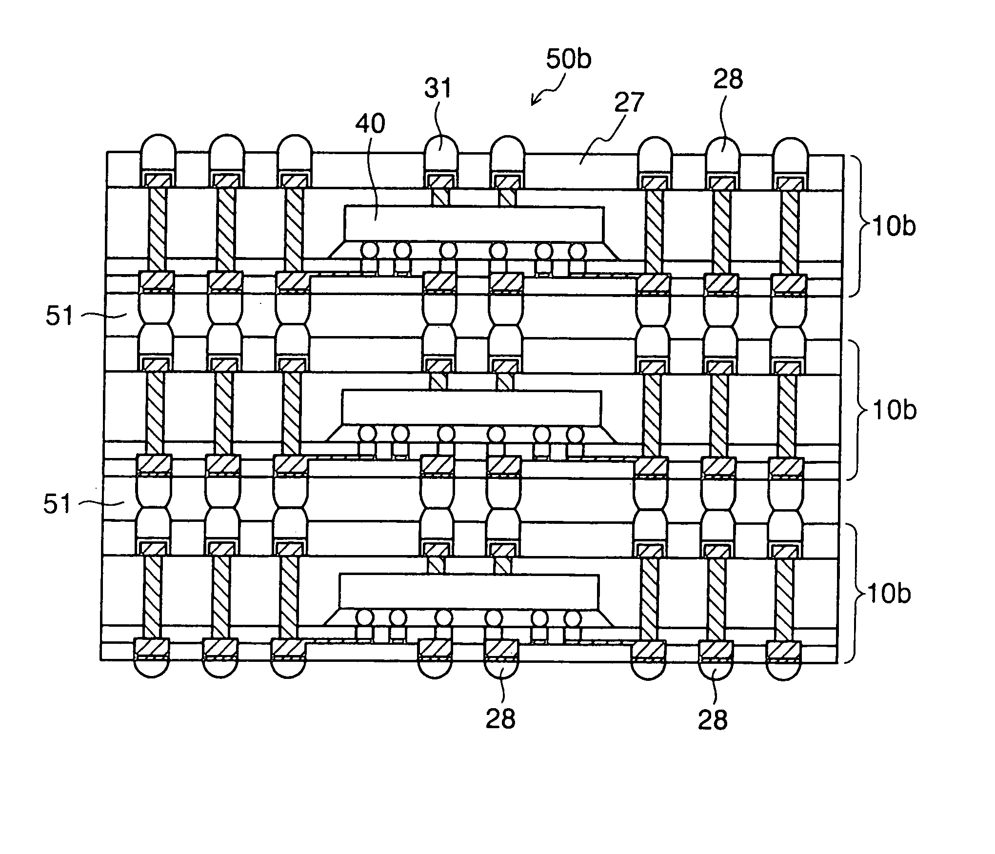
[0067] In this embodiment, similar to the second embodiment (FIG. 4), the semiconductor device 10b includes a wiring board 20b used as a package, and the semiconductor chip 40 buried in this package (wiring board) 20b. The package (wiring board) 20b in this embodiment differs from the package (wiring board) 20a in the second embodiment in the following points: heat spreading via holes (thermal vias) TH are formed in the resin layer 21 to communicate with the surface of the semiconductor chip 40 which is opposite to the surface having the electrode terminals 41 formed thereon; and the thermal vias TH are filled with the conductors 22 as thermally conductive bodies, and furthermore, the pad portions 24P (Ni / Au layer 25) on the conductors 22 are exposed from the solder resist layer 27 or covered with the exposed solder bumps 31 as thermally conductive bodies. Other ...


PUM


Abstract

In a semiconductor device, via holes are formed around a chip buried in a package, and conductor layers are respectively formed to be connected to one end and another end of the conductor filled in the individual via hole. Portions (pad portions) of the conductor layers which correspond to the conductors are exposed from protective films, or external connection terminals are bonded to the pad portions. The chip is mounted with flip-chip technology so that at least some of electrode terminals thereof are electrically connected to the conductor layers.

Description

CROSS-REFERENCE TO RELATED APPLICATIONS [0001] This application is based on and claims priority of Japanese Patent Application No. 2004-022581 filed on Jan. 30, 2004, the entire contents of which are incorporated herein by reference. BACKGROUND OF THE INVENTION [0002] (a) Field of the Invention [0003] The present invention relates to a semiconductor device and a method of manufacturing the same. More specifically, the present invention relates to a semiconductor device having a package structure in which a semiconductor element (chip) is mounted inside a wiring board for a reduction in thickness, and relates to a method of manufacturing the same. [0004] (b) Description of the Related Art [0005] Heretofore, semiconductor devices having various forms have been proposed in which a chip is mounted inside a wiring board. As an example thereof, there is a package structure (semiconductor device) intended to form a required circuit block by incorporating and stacking a plurality of chips, ...

Claims


Application Information

Patent Timeline
IPC IPC(8): H01L21/68H01L23/12H01L23/367H01L23/495H01L23/498H01L23/538H01L25/10H01L25/11H01L25/18
CPCH01L21/6835H01L2924/15192H01L23/49805H01L23/5389H01L24/73H01L24/91H01L25/105H01L2221/68345H01L2224/73204H01L2924/01002H01L2924/01003H01L2924/01015H01L2924/01029H01L2924/01046H01L2924/01078H01L2924/01079H01L2924/15311H01L2924/15331H01L2924/30105H01L2924/30107H01L2924/01005H01L2924/01006H01L2924/01033H01L23/3677H01L2224/81005H01L2224/73253H01L2924/10253H01L2225/1058H01L2225/1035H01L2224/32225H01L2224/16225H01L2924/00H01L2924/12042
Inventor TAKEUCHI, YUKIHARUTAKAYANAGI, HIDENORI
Owner SHINKO ELECTRIC IND CO LTD
Why Eureka
Try Eureka