Low cost three-dimensional memory array

a three-dimensional memory array and low-cost technology, applied in the field of low-cost three-dimensional memory arrays, can solve the problems of large devices giving rise to relatively large memory cells, high cost of memory chips, and need relative large switching devices, so as to reduce cost, reduce manufacturing costs, and reduce chip area

Inactive Publication Date: 2003-02-04
SANDISK TECH LLC
View PDF20 Cites 231 Cited by
  • Summary
  • Abstract
  • Description
  • Claims
  • Application Information

AI Technical Summary

Benefits of technology

Because the read current is relatively small, small memory cells occupying a small chip area may be used. In this way manufacturing costs are minimized. The disclosed memory arrays are well-suited for use in applications that can tolerate longer-than-conventional read access times, and for which the dramatic cost reduction that is achieved is particularly attractive.
Other preferred embodiments described below include a three-dimensional memory array having multiple vertically stacked layers of memory cells, each memory cell having a respective antifuse layer. The memory cells are characterized by an average maximum read current of less than 500 microamperes when the respective antifuse layers are disrupted. The memory cells also include first and second diode components, each characterized by a dopant concentration greater than 10.times.10.sup.19 / cm.sup.3. Boron dopant concentrations of 1.times.10.sup.20 / cm.sup.3 and 5.times.10.sup.20 / cm.sup.3 are disclosed. These high dopant levels provide the advantage of higher maximum read currents for a programmed memory cell.

Problems solved by technology

Unfortunately, to produce these relatively large read currents, relatively large switching devices are needed, and the large devices give rise to relatively large memory cells.
Large memory cells cause the memory chip area to be large, which means the memory chip cost will be high (since the cost increases as the area grows).

Method used


Image

  • Low cost three-dimensional memory array
  • Low cost three-dimensional memory array
  • Low cost three-dimensional memory array

Examples


Embodiment Construction

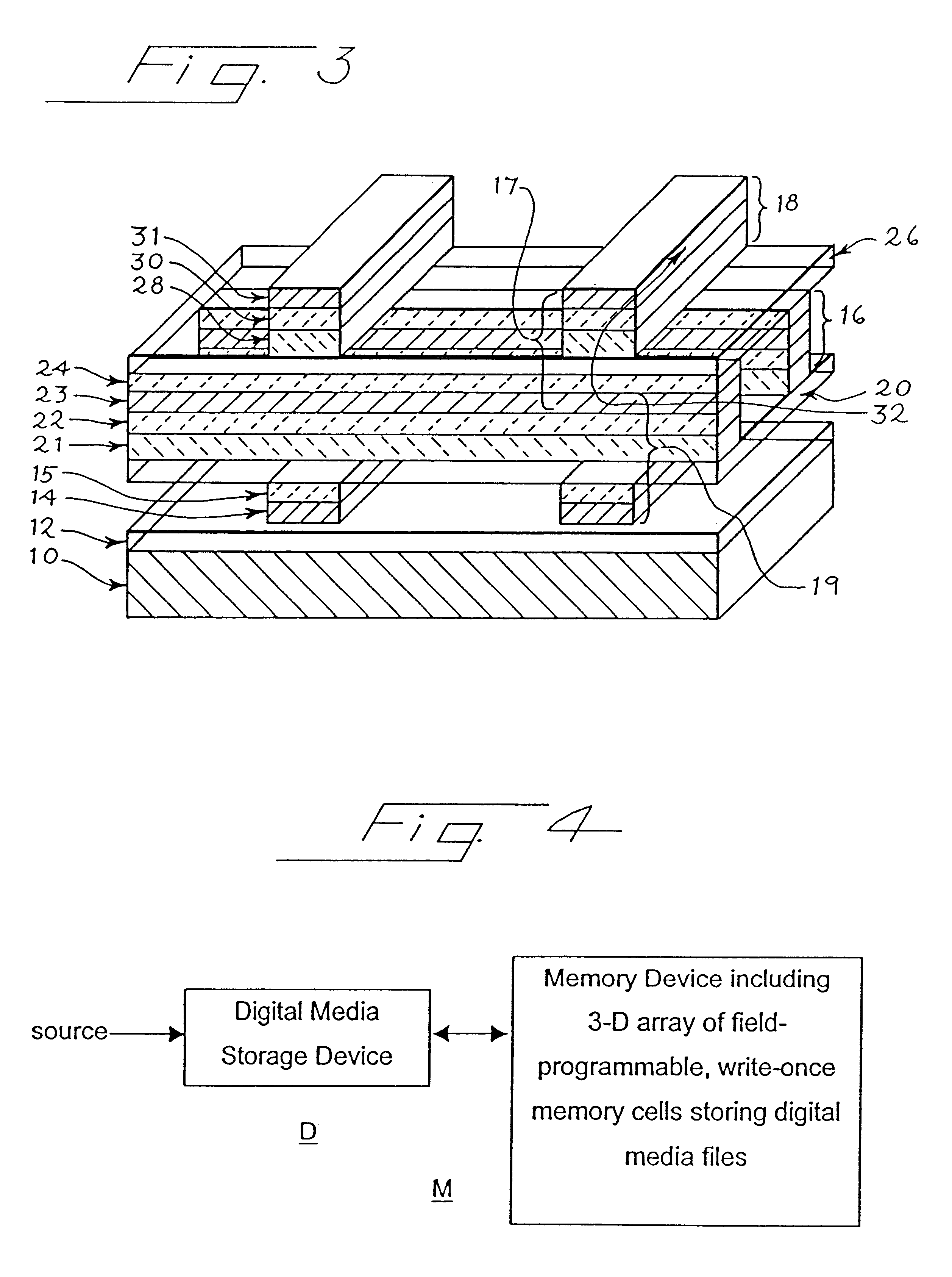
A low-cost, three-dimensional memory array is described. In the following description, numerous specific details are set forth such as specific materials and layer thicknesses. It will be apparent, however, to one skilled in the art that the present invention may be practiced without these details. In other instances, well-known circuits and fabrication techniques have not been set forth in detail in order not to unnecessarily obscure the present invention.

General Discussion

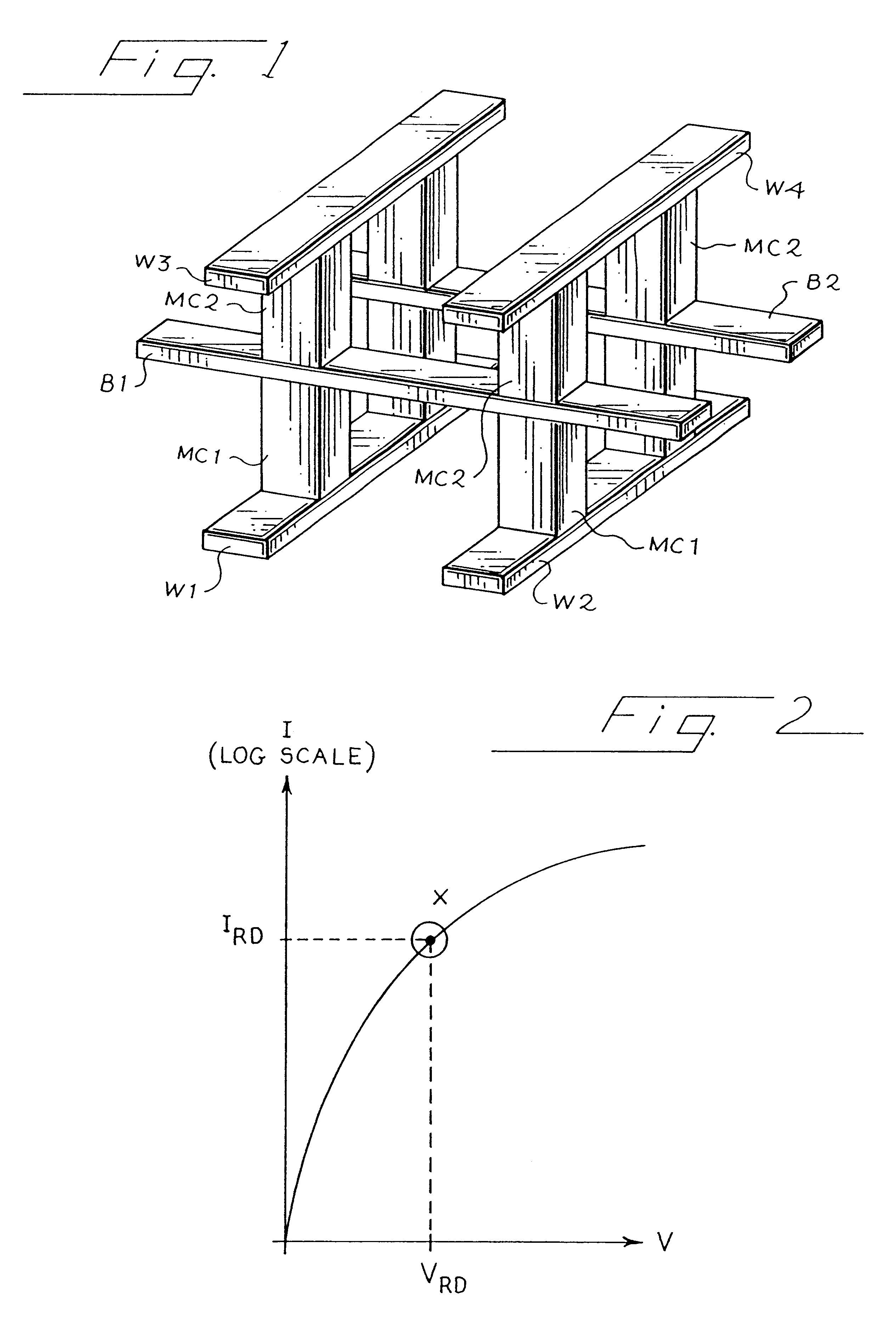
In the embodiments described below, memory cells are organized and built in three dimensions rather than two. There are several layers of memory cells, and the layers are vertically stacked above one another. The three dimensions are called "rows", "columns", and "layers". Typically, the rows and columns are generally parallel to the upper surface of an underlying substrate, and the layers are separated from one another along a direction perpendicular to the upper surface of the underlying substrate.

Some memory c...


PUM


Abstract

A low-cost memory cell array includes multiple, vertically-stacked layers of memory cells. In one form, each memory cell is characterized by a small cross-sectional area and a read current less than 6.3 microamperes. The resulting memory array has a slow access time and is well-suited for digital media storage, where access time requirements are low and the dramatic cost reductions associated with the disclosed memory arrays are particularly attractive. In another form, each memory cell includes an antifuse layer and diode components, wherein at least one diode component is heavily doped (to a dopant concentration greater than 1019 / cm3), and wherein the read current is large (up to 500 mA).

Description

This invention relates to three-dimensional memory arrays of the type that include multiple vertically-stacked layers of memory cells, and in particular to such memory arrays that are particularly low in manufacturing cost.The marketplace is demanding memory chips containing an ever-larger number of storage bits, at an ever-lower cost per bit. It is extremely desirable to provide a high-capacity memory at a very low cost, to serve this expanding market.Conventional memory design assumes that high-speed read access is an important goal. The basic memory cell is conventionally designed to provide a relatively large read current, ensuring a relatively fast read access. Unfortunately, to produce these relatively large read currents, relatively large switching devices are needed, and the large devices give rise to relatively large memory cells. Large memory cells cause the memory chip area to be large, which means the memory chip cost will be high (since the cost increases as the area gr...

Claims


Application Information

Patent Timeline
Patent Type & Authority Patents(United States)
IPC IPC(8): G11C17/14G11C17/16H01L27/10H01L27/06
CPCG11C17/16H01L27/101H01L27/0688
Inventor JOHNSON, MARK G.LEE, THOMAS H.SUBRAMANIAN, VIVEKFARMWALD, P. MICHAELKNALL, N. JOHAN
Owner SANDISK TECH LLC
Why Eureka
Try Eureka