Semiconductor wafer with well contacts on back side

Inactive Publication Date: 2005-03-08
XILINX INC
View PDF13 Cites 241 Cited by
  • Summary
  • Abstract
  • Description
  • Claims
  • Application Information

AI Technical Summary

Benefits of technology

A supporting structure such as a silicon wafer is wafer-bonded to the upper face side of a partially processed or fully processed device wafer. The device wafer includes a field effect MOS transistor. The field e

Problems solved by technology

In MOS transistors such as the transistors of FIG. 1, switching speed is limited by the time required to charge and discharge the capacitances between device electrodes.
In addition to transistors 2 and 7 of FIG. 1 being slowed due to the presence of parasitic junction capacitances, the performance of transistors 2 and 7 also suffers due to a resistance existing between the well contact and the channel of each transistor.
In addition to currents flowing past the channel region of a transistor due to alpha particles, the normal switching of the transistors can also cause undesirable currents to flow in the transistor

Method used


Image

  • Semiconductor wafer with well contacts on back side
  • Semiconductor wafer with well contacts on back side
  • Semiconductor wafer with well contacts on back side

Examples


Embodiment Construction

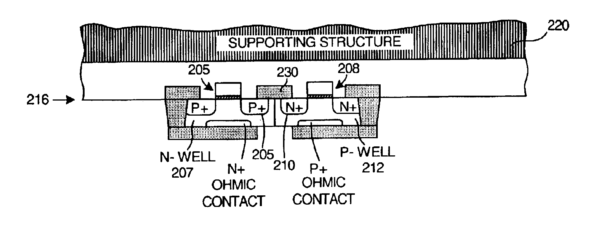
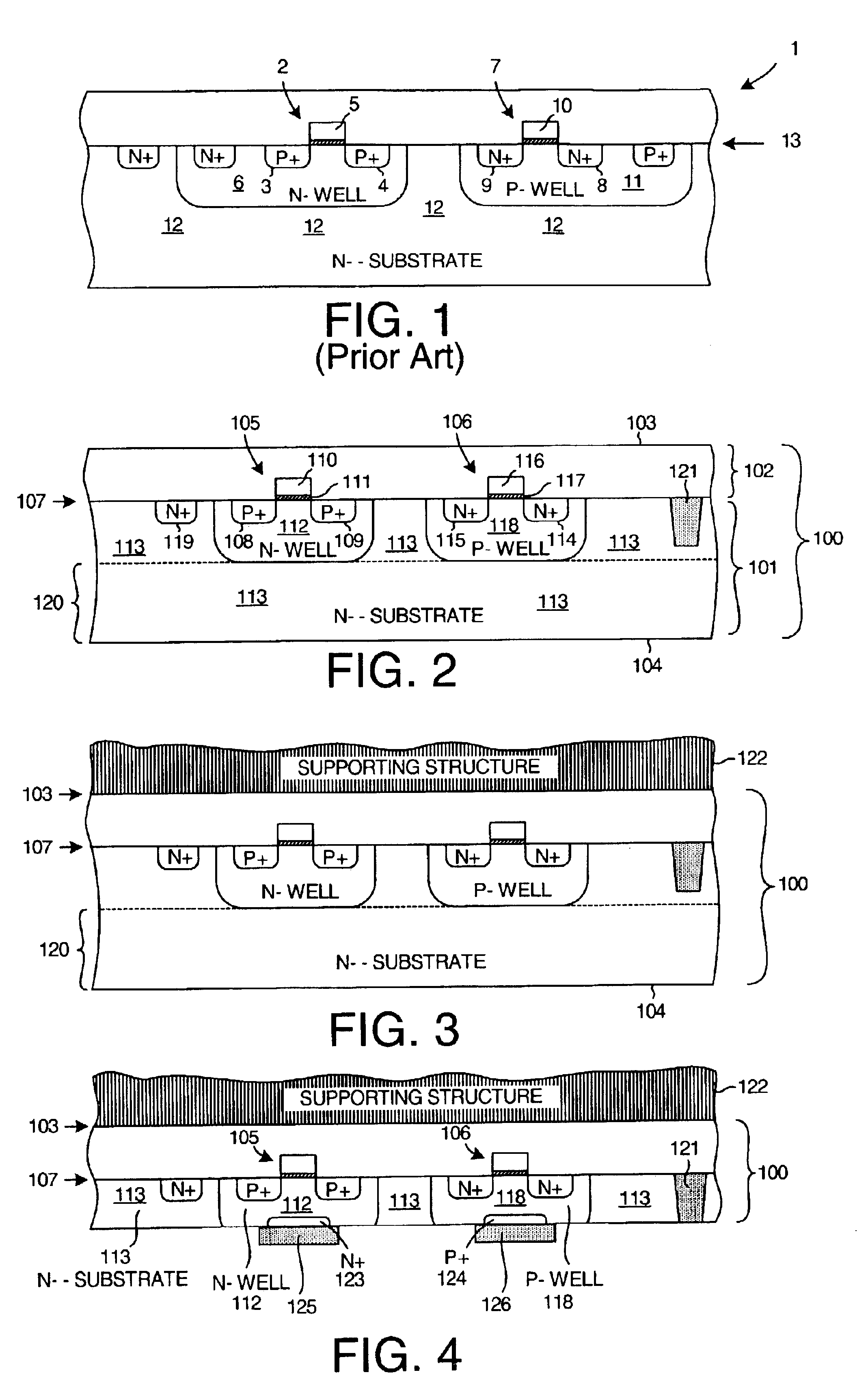
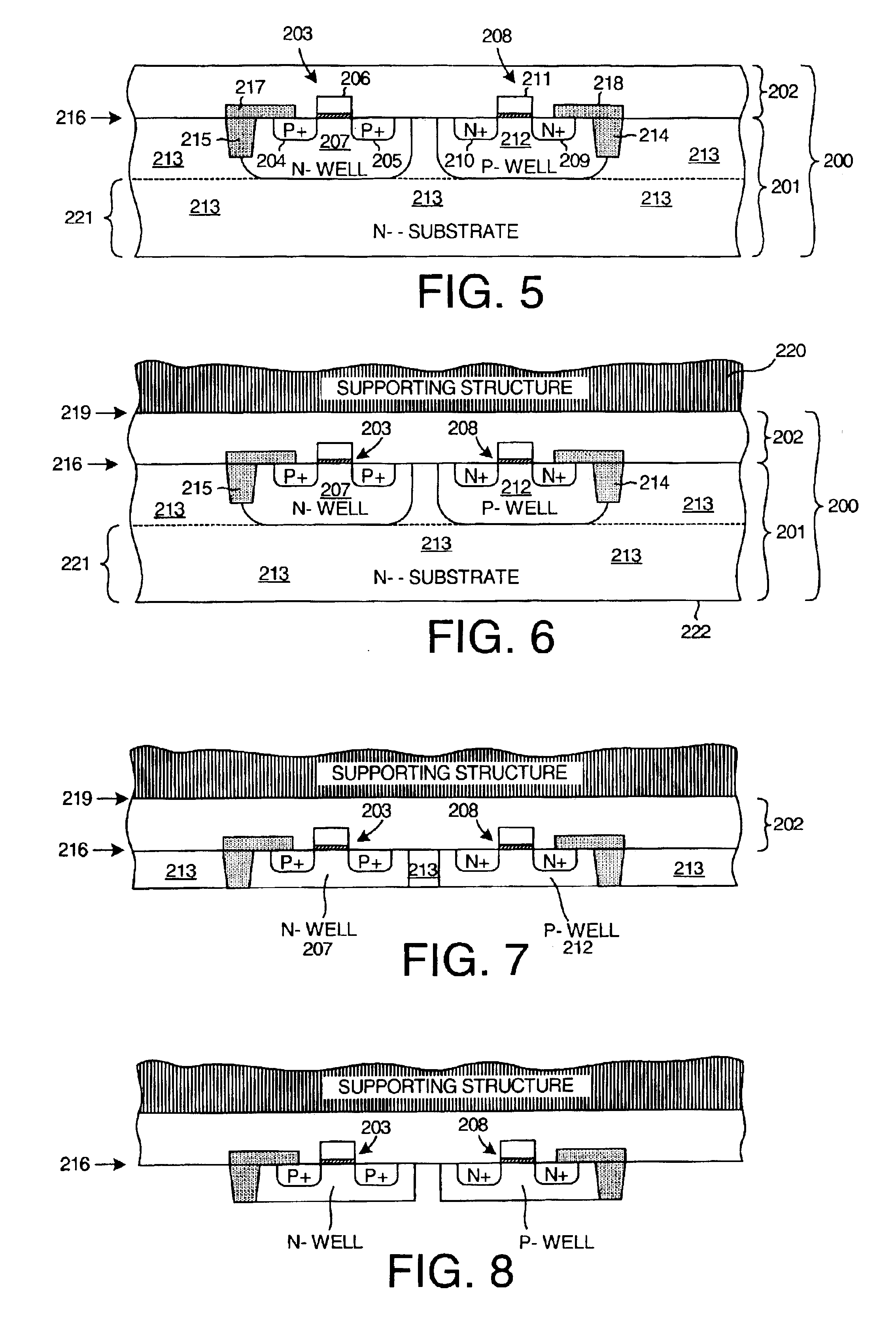
FIG. 2 is a simplified cross-sectional diagram of a device wafer 100 in an initial step of a first method. Device wafer 100 includes a semiconductor wafer portion 101 and an overlying interconnect portion 102. Device wafer 100 has an upper face side surface 103 and a back side surface 104. Device wafer 100 is, in this example, a wafer of monocrystalline silicon.

A first transistor 105 and a second transistor 106 are formed on and into an upper surface 107 of the semiconductor wafer portion 101 of device wafer 100. First transistor 105 is a P-channel MOS field effect transistor having a P-type source region 108, a P-type drain region 109, and a gate 110. A channel region exists between source region 108 and drain region 109. A thin thermal oxide gate insulating layer 111 separates gate 110 from the underlying channel region. The source and drain regions 108 and 109 are regions of diffusion that extend down into an N-type well region 112. N-type well region 112 is made smaller in the l...


PUM


Abstract

A supporting structure is wafer-bonded to the upper face side of a partially or fully processed device wafer. The device wafer includes a transistor having a well region that extends into the substrate material of the device wafer. The source and drain regions of the transistor extend into the well region. After attachment of the supporting structure, the device wafer is thinned from the back side until the bottom of the well region is reached. To reduce source and drain junction capacitances, etching can continue until the source and drain regions are reached. In one embodiment, all of the well-to-substrate junction is removed in a subsequent etching step, thereby reducing or eliminating the well-to-substrate junction capacitance of the resulting transistor. Resistance between the well electrode and the transistor channel is reduced because the well contact is disposed on the back side of the device wafer directly under the gate of the transistor.

Description

FIELD OF THE INVENTIONThe present invention relates to bond and etchback semiconductor-on-insulator (BESOI) semiconductor processing technology and related structures.BACKGROUND INFORMATIONFIG. 1 (Prior Art) is a cross-sectional diagram of a conventional complementary metal oxide semiconductor (CMOS) transistor structure 1 often used in contemporary ultra large scale integration. The diagram is simplified to better illustrate the related issues. Structure 1 includes a P-channel transistor 2 having a source region 3, a drain region 4 and a gate 5. A channel region exists between source region 3 and drain region 4. Source region 3 and drain region 4 extend into in an N-type well region 6.The structure also includes an N-channel transistor 7 having a source region 8, a drain region 9 and a gate 10. A channel region exists between source region 8 and drain region 9. Source region 8 and drain region 9 extend into in a P-type well region 11. Well regions 6 and 11 are diffused into a bulk ...

Claims


Application Information

Patent Timeline
IPC IPC(8): H01L21/02H01L21/30H01L21/20H01L21/306H01L21/8238H01L27/092H01L27/12
CPCH01L21/2007H01L21/823871H01L27/0928H01L21/823892H01L27/12
Inventor CONN, ROBERT O.
Owner XILINX INC
Why Eureka
Try Eureka